

Comparing X-ray Diffraction And SEM: Practical Insights
FEB 27, 20269 MIN READ
Generate Your Research Report Instantly with AI Agent
Patsnap Eureka helps you evaluate technical feasibility & market potential.
X-ray Diffraction and SEM Technology Background and Objectives
X-ray diffraction (XRD) and scanning electron microscopy (SEM) represent two fundamental analytical techniques that have revolutionized materials characterization since their development in the early 20th century. XRD emerged from the pioneering work of Max von Laue and the Bragg father-son duo between 1912-1913, establishing the foundation for crystallographic analysis through the interaction of X-rays with crystalline materials. SEM technology followed several decades later, with the first commercial instruments appearing in the 1960s, building upon electron optics principles developed in the 1930s.
The evolution of these technologies has been driven by the increasing demand for precise materials characterization across multiple industries. XRD has progressed from simple powder diffraction cameras to sophisticated automated diffractometers capable of real-time analysis, while SEM has advanced from basic imaging systems to high-resolution instruments with sub-nanometer capabilities and integrated analytical features.
Both techniques serve complementary roles in modern materials science, addressing the critical need for comprehensive structural and morphological analysis. XRD excels in providing quantitative crystallographic information, including phase identification, crystal structure determination, and lattice parameter measurements. Its non-destructive nature and ability to analyze bulk materials make it indispensable for quality control and research applications.
SEM technology focuses on surface morphology and microstructural analysis, offering exceptional spatial resolution and depth of field. The integration of energy-dispersive X-ray spectroscopy (EDS) and other analytical techniques has expanded SEM capabilities to include elemental mapping and compositional analysis.
The primary objective of comparing these technologies lies in understanding their respective strengths and limitations to optimize analytical workflows. XRD provides statistically representative bulk information but lacks spatial resolution, while SEM offers detailed local information with limited sampling volume. Modern analytical challenges require strategic combination of both techniques to achieve comprehensive materials characterization.
Current technological objectives focus on enhancing automation, reducing analysis time, and improving data correlation between XRD and SEM results. Advanced software integration and machine learning algorithms are being developed to streamline comparative analysis and extract maximum information from combined datasets, ultimately enabling more informed materials development decisions.
Market Demand for Advanced Material Characterization Techniques
The global market for advanced material characterization techniques is experiencing unprecedented growth driven by the increasing complexity of modern materials and the demand for precise analytical capabilities. Industries ranging from semiconductor manufacturing to pharmaceutical development require sophisticated characterization methods to understand material properties at micro and nanoscale levels. This demand has positioned X-ray diffraction and scanning electron microscopy as critical analytical tools across multiple sectors.
Semiconductor and electronics industries represent the largest market segment for these characterization techniques. The continuous miniaturization of electronic components and the development of novel materials such as two-dimensional materials and quantum dots necessitate advanced analytical capabilities. Both XRD and SEM technologies are essential for quality control, failure analysis, and research and development activities in these sectors. The growing adoption of electric vehicles and renewable energy technologies further amplifies the demand for battery material characterization and solar cell analysis.
The pharmaceutical and biotechnology sectors constitute another significant market driver. Drug development processes require comprehensive understanding of crystalline polymorphs, particle size distributions, and surface morphologies. XRD provides crucial information about crystal structures and phase purity, while SEM offers detailed morphological analysis essential for formulation development and quality assurance. The increasing focus on personalized medicine and novel drug delivery systems has expanded the application scope of these techniques.
Materials science research institutions and academic laboratories form a substantial portion of the market demand. The development of advanced materials such as metal-organic frameworks, nanocomposites, and biomaterials requires sophisticated characterization capabilities. Government funding for materials research and the establishment of national laboratories focused on advanced manufacturing have contributed to sustained market growth.
The automotive and aerospace industries are emerging as significant consumers of advanced characterization techniques. Lightweight materials, advanced alloys, and composite materials used in these industries require thorough characterization to ensure safety and performance standards. The shift toward sustainable manufacturing practices has increased the demand for material recycling and lifecycle analysis, further driving the need for comprehensive characterization capabilities.
Market trends indicate a growing preference for integrated analytical solutions that combine multiple characterization techniques. Users increasingly seek platforms that can provide complementary information from both XRD and SEM analyses within unified workflows. This trend has influenced instrument manufacturers to develop hybrid systems and software solutions that facilitate comparative analysis and data correlation between different characterization methods.
Current State and Challenges in XRD and SEM Applications
X-ray diffraction and scanning electron microscopy represent two cornerstone analytical techniques in materials characterization, each experiencing significant technological advancement while facing distinct operational challenges. XRD technology has evolved from conventional powder diffractometers to high-resolution synchrotron-based systems, enabling unprecedented structural analysis capabilities. Modern XRD instruments incorporate advanced detector technologies, automated sample handling systems, and sophisticated software for phase identification and quantitative analysis.
SEM technology has similarly progressed from basic thermionic emission systems to field emission guns with sub-nanometer resolution capabilities. Environmental SEM variants now allow observation of samples under controlled atmospheric conditions, while cryo-SEM enables analysis of hydrated biological specimens. The integration of focused ion beam technology with SEM has created dual-beam systems for precise sample preparation and three-dimensional analysis.
Despite these advances, both techniques face significant operational constraints. XRD analysis remains limited by crystalline sample requirements, with amorphous materials presenting interpretation challenges. Sample preparation protocols often require extensive grinding and mounting procedures, potentially introducing artifacts. Peak overlap in complex multi-phase systems continues to complicate quantitative analysis, particularly when dealing with nanocrystalline materials where peak broadening effects become pronounced.
SEM applications encounter different but equally challenging limitations. Beam damage remains a critical concern for organic and beam-sensitive materials, requiring careful optimization of acceleration voltages and exposure times. Charging effects in non-conductive samples necessitate coating procedures that may obscure surface features or alter chemical composition. Sample preparation artifacts, including dehydration effects and coating thickness variations, can significantly impact imaging quality and analytical accuracy.
Current technological gaps include limited real-time analysis capabilities for both techniques. XRD measurements typically require extended acquisition times for high-quality data, while SEM imaging demands careful manual optimization for each sample region. Integration challenges persist when combining these complementary techniques, as sample preparation requirements often differ significantly between methods.
The geographical distribution of advanced instrumentation remains concentrated in developed regions, with emerging markets facing accessibility barriers due to high capital costs and maintenance requirements. This disparity limits global research capabilities and collaborative potential in materials science applications.
Current XRD and SEM Analysis Solutions
01 Combined use of X-ray diffraction and SEM for material characterization
X-ray diffraction (XRD) and scanning electron microscopy (SEM) are complementary analytical techniques used together to comprehensively characterize materials. XRD provides information about crystalline structure, phase composition, and lattice parameters, while SEM offers detailed surface morphology and microstructural analysis. The combination of these techniques enables researchers to correlate structural properties with surface features, providing a complete understanding of material properties at both atomic and microscopic scales.- Combined use of X-ray diffraction and SEM for material characterization: X-ray diffraction (XRD) and scanning electron microscopy (SEM) are complementary analytical techniques used together to comprehensively characterize materials. XRD provides information about crystalline structure, phase composition, and lattice parameters, while SEM offers detailed surface morphology and microstructural analysis. The combination of these techniques enables researchers to correlate structural properties with surface features, providing a complete understanding of material properties at both atomic and microscopic scales.
- Application in powder and particle analysis: These analytical methods are extensively employed for examining powder materials and particulate systems. The techniques allow for determination of particle size distribution, crystallinity, and surface characteristics. This approach is particularly valuable in pharmaceutical, ceramic, and metallurgical applications where particle properties directly influence product performance and quality control requirements.
- Thin film and coating characterization: The combined techniques are utilized for analyzing thin films and surface coatings to determine film thickness, crystallographic orientation, grain structure, and surface uniformity. This characterization is critical in semiconductor manufacturing, optical coatings, and protective layer applications where precise control of film properties is essential for device performance and durability.
- Composite and multi-phase material analysis: These techniques are applied to investigate composite materials and multi-phase systems to identify different phases, their distribution, and interfacial characteristics. The methods enable determination of phase composition, crystallographic relationships between phases, and spatial distribution of components. This is particularly important in advanced materials development, including metal matrix composites, ceramic composites, and hybrid materials.
- Quality control and defect detection: The integration of these analytical methods serves as a powerful quality control tool for detecting defects, impurities, and structural anomalies in manufactured products. The techniques can identify crystallographic defects, surface irregularities, contamination, and deviations from desired specifications. This application is crucial in manufacturing processes across various industries to ensure product consistency and reliability.
02 Application in powder and particle analysis
These analytical methods are extensively employed for examining powder materials and particulate systems. The techniques allow for determination of particle size distribution, crystallinity, and surface characteristics. This approach is particularly valuable in pharmaceutical, ceramic, and metallurgical applications where particle properties directly influence product performance and quality control.Expand Specific Solutions03 Thin film and coating characterization
The combined techniques are utilized for analyzing thin films and surface coatings to determine film thickness, crystallographic orientation, grain structure, and surface uniformity. This application is critical in semiconductor manufacturing, optical coatings, and protective layer development where precise control of film properties is essential for device performance.Expand Specific Solutions04 Composite and multi-phase material analysis
These techniques are applied to investigate composite materials and multi-phase systems to identify different phases, their distribution, and interfacial characteristics. The methods enable determination of phase composition, crystal structure of individual components, and spatial arrangement of phases within the material matrix, which is crucial for understanding mechanical and functional properties of advanced materials.Expand Specific Solutions05 Quality control and defect detection in manufacturing
Both analytical techniques serve as powerful tools for quality assurance and defect identification in manufacturing processes. They can detect structural defects, contamination, phase transformations, and surface irregularities that may affect product performance. This application is widely used across industries including electronics, automotive, and materials production to ensure product consistency and identify process deviations.Expand Specific Solutions
Key Players in XRD and SEM Equipment Industry
The X-ray diffraction and SEM comparison technology landscape represents a mature analytical instrumentation market experiencing steady growth driven by semiconductor, materials science, and nanotechnology applications. The industry is in a consolidation phase with established players dominating through technological differentiation and comprehensive service offerings. Market size exceeds several billion dollars globally, supported by increasing demand for advanced characterization techniques in R&D and quality control. Technology maturity varies significantly between segments, with companies like FEI Co., JEOL Ltd., and Applied Materials leading SEM innovations, while Panalytical and Bruker Nano advance X-ray diffraction capabilities. Hitachi, Carl Zeiss X-ray Microscopy, and KLA Corp. demonstrate strong integration of both technologies. Emerging players like ELDICO Scientific AG are pioneering electron diffraction crystallography, indicating continued innovation potential. The competitive landscape shows high barriers to entry due to substantial R&D investments and established customer relationships, with market leaders maintaining positions through continuous technological advancement and strategic acquisitions.
FEI Co.
Technical Solution: FEI develops integrated X-ray diffraction and SEM solutions through their dual-beam systems that combine focused ion beam (FIB) and electron microscopy capabilities. Their approach enables correlative analysis where XRD provides crystallographic information about phase identification and crystal structure, while SEM offers high-resolution morphological imaging. The company's Helios series integrates these techniques for comprehensive materials characterization, allowing researchers to perform site-specific sample preparation and analysis. This integration is particularly valuable for failure analysis and materials research where both structural and morphological information are critical for understanding material properties and behavior.
Strengths: Excellent integration of multiple analytical techniques in single platform, high precision sample preparation capabilities. Weaknesses: High equipment cost and complexity, requires specialized operator training for optimal performance.
JEOL Ltd.
Technical Solution: JEOL offers comprehensive solutions combining X-ray diffraction and scanning electron microscopy through their integrated analytical systems. Their approach focuses on correlative microscopy where XRD provides crystallographic data for phase identification and quantitative analysis, while SEM delivers detailed surface morphology and compositional information through energy-dispersive spectroscopy (EDS). JEOL's systems feature automated sample handling and positioning systems that enable seamless transition between XRD and SEM analysis on the same sample area. Their software platforms provide integrated data analysis capabilities that correlate structural and morphological findings, enhancing materials characterization workflows in semiconductor, pharmaceutical, and materials science applications.
Strengths: Strong automation capabilities and user-friendly interfaces, excellent technical support and training programs. Weaknesses: Limited customization options compared to modular systems, higher maintenance requirements for integrated platforms.
Core Innovations in Comparative XRD-SEM Methodologies
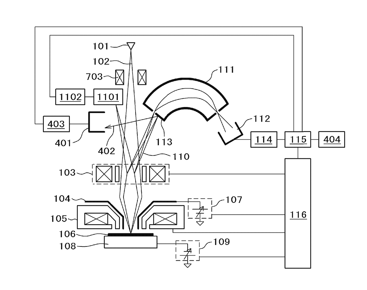
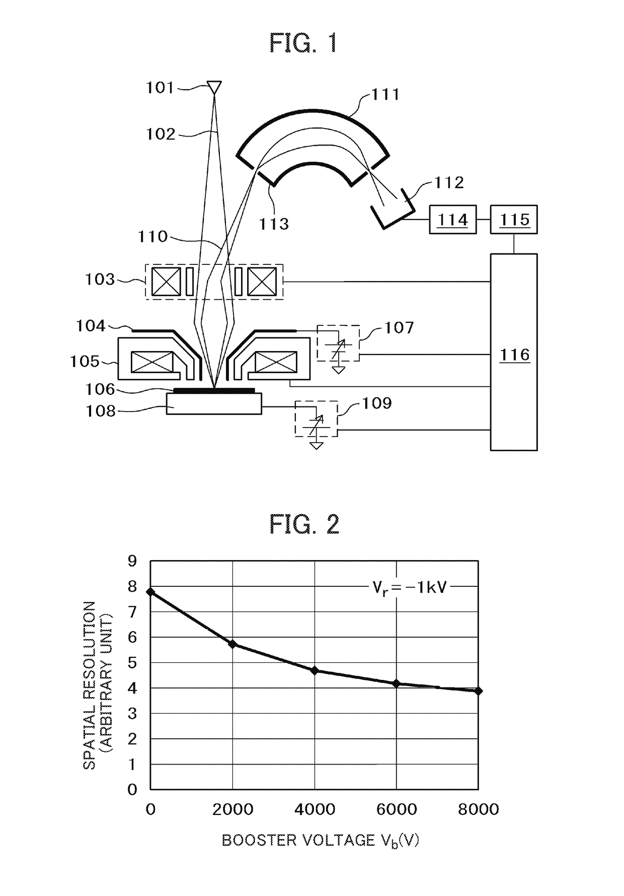
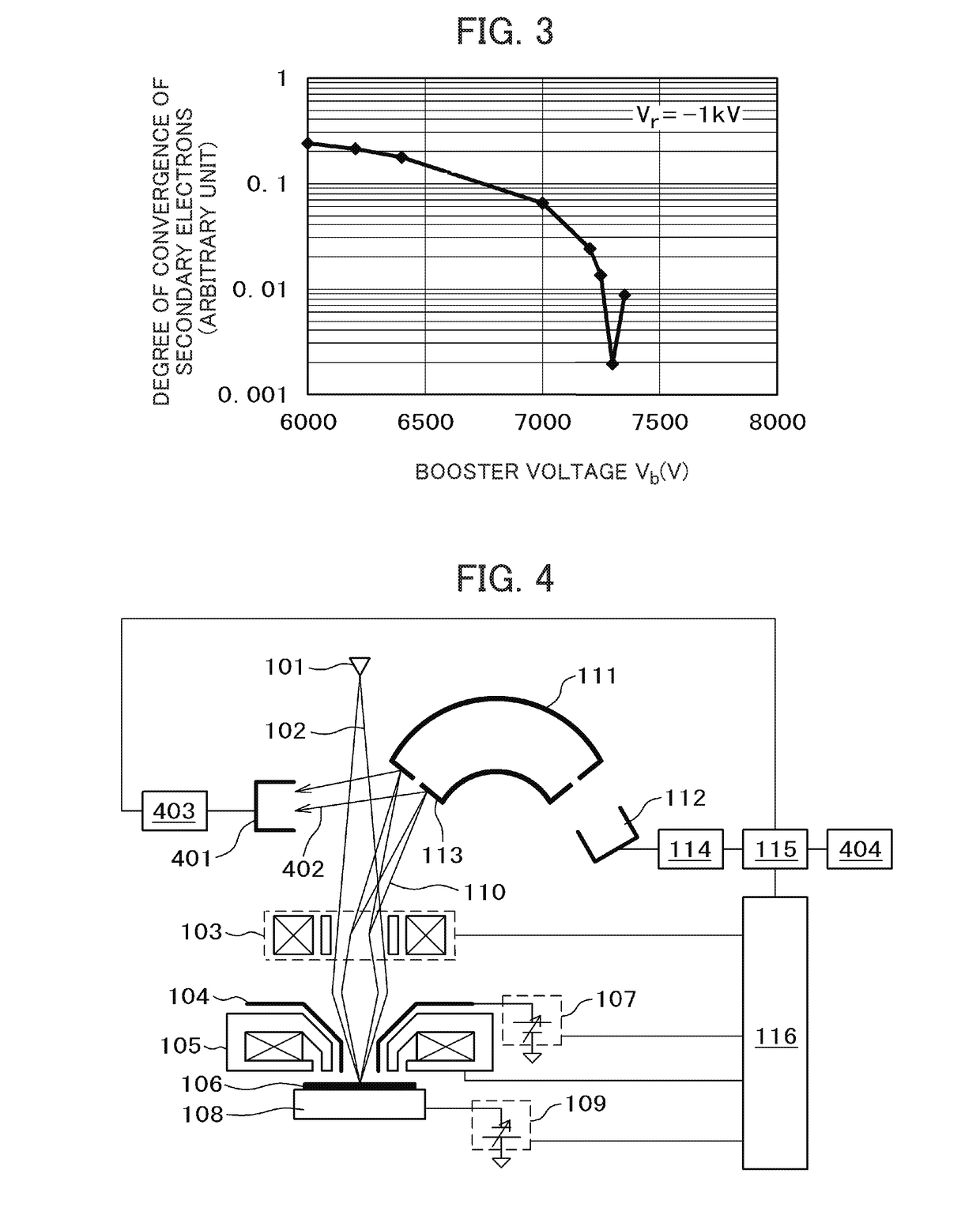
Scanning electron microscope and electron trajectory adjustment method therefor
PatentActiveUS20170263415A1
Innovation
- The implementation of a scanning electron microscope system that includes an electron source, objective lens, primary electron acceleration and deceleration means, a secondary electron deflector, spectroscope, and detectors, with a controller to optimize voltage settings for the objective lens and electron acceleration/deceleration means to converge secondary electrons effectively into the spectroscope, enhancing spatial resolution and detection rates.

Electron microscope
PatentActiveUS20150144787A1
Innovation
- An electron microscope configuration using a single electromagnet to provide the functions of three electron-optical lenses, allowing for the imaging of the diffraction plane at a detector without a separate projection system, with adjustable magnetic fields to focus and magnify the electron beam, enabling the detection of both bright and dark field electrons.


Sample Preparation Standards and Quality Control
Sample preparation represents the most critical factor determining the reliability and accuracy of both X-ray diffraction and scanning electron microscopy analyses. The quality of analytical results directly correlates with adherence to established preparation protocols, making standardization essential for meaningful comparative studies between these complementary techniques.
For XRD applications, sample preparation standards emphasize achieving optimal particle size distribution, typically requiring grinding to sub-10 micrometer particles to minimize preferred orientation effects. The preparation process must ensure representative sampling while avoiding contamination from grinding media. Standard protocols mandate specific loading techniques for powder diffractometers, including back-loading methods and the use of zero-background holders to eliminate substrate interference.
SEM sample preparation follows distinctly different quality control parameters, focusing primarily on surface preservation and conductivity enhancement. Standard protocols require careful attention to mounting procedures, with conductive carbon or metal tabs ensuring proper electrical grounding. For non-conductive samples, sputter coating with gold, platinum, or carbon becomes mandatory, with thickness control typically maintained between 5-20 nanometers to preserve surface morphology while providing adequate conductivity.
Cross-contamination prevention emerges as a paramount concern when samples undergo preparation for both techniques sequentially. Quality control measures include dedicated preparation areas, separate grinding equipment, and thorough cleaning protocols between samples. Documentation standards require detailed preparation logs, including grinding times, coating parameters, and storage conditions to ensure reproducibility.
Environmental control during preparation significantly impacts both techniques. Humidity control prevents hydration artifacts in XRD patterns, while temperature stability ensures consistent coating quality for SEM specimens. Standard operating procedures mandate controlled atmosphere storage for prepared samples, particularly those sensitive to oxidation or moisture absorption.
Quality assessment protocols incorporate reference materials and control samples to validate preparation effectiveness. For XRD, silicon powder standards verify instrumental alignment and sample preparation consistency. SEM preparation quality relies on resolution test specimens and coating thickness measurements using quartz crystal monitors or ellipsometry techniques.
Sample preservation standards address the temporal stability of prepared specimens. XRD samples require protection from atmospheric moisture and temperature fluctuations, while SEM specimens demand vacuum storage to prevent coating degradation and contamination accumulation. These preservation protocols ensure analytical consistency across extended measurement campaigns and enable reliable inter-technique comparisons.
Cost-Benefit Analysis of XRD vs SEM Implementation
The implementation of X-ray Diffraction (XRD) and Scanning Electron Microscopy (SEM) systems requires substantial capital investment, with costs varying significantly based on instrument specifications and intended applications. Entry-level XRD systems typically range from $150,000 to $300,000, while high-resolution research-grade instruments can exceed $500,000. SEM systems demonstrate broader cost variation, with tabletop models starting around $100,000 and high-end field emission systems reaching $1.5 million or more.
Operational expenses constitute a critical component of total ownership costs. XRD systems generally require lower maintenance due to fewer mechanical components, with annual service contracts typically ranging from 8-12% of initial purchase price. Sample preparation costs remain minimal, often requiring only basic grinding and mounting procedures. SEM systems demand higher operational investment, including specialized sample preparation facilities, coating equipment, and controlled environmental conditions. Annual maintenance contracts typically represent 10-15% of initial investment, with additional costs for electron gun replacements and vacuum system maintenance.
Personnel requirements differ substantially between technologies. XRD operation can often be managed by technicians with moderate training, requiring approximately 40-80 hours of initial instruction. SEM systems demand more extensive operator training, typically requiring 120-200 hours for proficiency development, particularly for advanced imaging techniques and sample preparation protocols.
Return on investment calculations must consider analytical throughput and revenue generation potential. XRD systems excel in high-throughput quantitative analysis, enabling processing of 20-50 samples daily for routine phase identification. This efficiency translates to lower per-sample analysis costs, typically ranging from $50-150 per measurement. SEM analysis generally requires longer examination periods, limiting daily throughput to 5-15 samples, with per-sample costs ranging from $100-400 depending on complexity.
The complementary nature of these techniques often justifies dual implementation in research and industrial environments. Organizations frequently achieve optimal cost-effectiveness by establishing XRD capabilities for routine crystallographic analysis while accessing SEM services through partnerships or outsourcing arrangements for specialized morphological investigations. This hybrid approach maximizes analytical capabilities while optimizing capital allocation and operational efficiency.
Unlock deeper insights with Patsnap Eureka Quick Research — get a full tech report to explore trends and direct your research. Try now!
Generate Your Research Report Instantly with AI Agent
Supercharge your innovation with Patsnap Eureka AI Agent Platform!