

Detector Materials For Room-Temperature Terahertz Sensing
AUG 29, 202510 MIN READ
Generate Your Research Report Instantly with AI Agent
PatSnap Eureka helps you evaluate technical feasibility & market potential.
THz Sensing Materials Background and Objectives
Terahertz (THz) radiation, occupying the spectral region between microwave and infrared frequencies (0.1-10 THz), has emerged as a frontier in sensing technology over the past three decades. This frequency range offers unique capabilities for non-destructive, non-ionizing imaging and spectroscopy with applications spanning security screening, medical diagnostics, quality control, and wireless communications. The development trajectory of THz technology has been marked by significant advancements in both radiation sources and detection materials, with the latter presenting persistent challenges for practical implementation.
Historically, THz detection required cryogenic cooling systems, severely limiting widespread adoption due to operational complexity and cost constraints. The pursuit of room-temperature THz sensing materials represents a critical inflection point in the technology's evolution, potentially enabling compact, energy-efficient, and commercially viable THz systems for everyday applications. This technological progression aligns with broader trends in materials science, where novel nanomaterials and heterostructures are enabling unprecedented sensing capabilities across the electromagnetic spectrum.
The primary objective in this field is to develop detector materials capable of efficient THz radiation absorption and signal transduction at ambient temperatures. Ideal materials must demonstrate high sensitivity, fast response times, broad spectral coverage, and stability under normal operating conditions. Additionally, compatibility with standard semiconductor fabrication processes represents a crucial consideration for eventual mass production and integration with existing electronic systems.
Current research focuses on several promising material platforms, including two-dimensional electron gas systems, graphene and other 2D materials, plasma-wave detectors based on field-effect transistors, and various nanostructured semiconductors. Each approach offers distinct advantages and limitations regarding sensitivity, frequency response, and fabrication complexity. The convergence of nanotechnology, materials science, and electronics engineering has accelerated innovation in this domain, with significant breakthroughs reported in recent literature.
Beyond material development, complementary objectives include miniaturization of detector arrays, reduction of power requirements, enhancement of signal-to-noise ratios, and integration with readout electronics. These technical goals are driven by market demands for portable, user-friendly THz sensing systems that can operate reliably outside laboratory environments. The ultimate vision encompasses affordable, room-temperature THz detectors that enable widespread adoption across industrial, medical, and consumer applications.
The achievement of these objectives would represent a transformative advancement in electromagnetic sensing technology, potentially unlocking numerous applications previously constrained by the "terahertz gap" – the historical difficulty in generating and detecting radiation in this frequency range. As global research efforts intensify, the realization of practical room-temperature THz sensing appears increasingly within reach, promising new capabilities in fields ranging from biomedical imaging to next-generation wireless communications.
Market Applications for Room-Temperature THz Detection
The terahertz (THz) sensing market is experiencing significant growth as room-temperature detection capabilities mature, opening numerous commercial and industrial applications previously limited by cryogenic cooling requirements. The global THz technology market is projected to reach $1.2 billion by 2025, with a compound annual growth rate exceeding 25% between 2020-2025, driven largely by advancements in room-temperature detector materials.
Security and defense sectors represent the largest current market application, accounting for approximately 30% of THz sensing deployments. Room-temperature THz detectors enable portable security screening systems for non-invasive detection of concealed weapons, explosives, and contraband at airports, borders, and high-security facilities. The ability to operate without cooling infrastructure significantly reduces system size, weight, power consumption, and maintenance requirements.
Medical diagnostics and healthcare applications constitute a rapidly expanding market segment. Room-temperature THz sensing enables non-ionizing, non-invasive imaging for early detection of skin cancer, dental caries, and burn assessment. The pharmaceutical industry increasingly utilizes THz spectroscopy for quality control in drug manufacturing, detecting chemical composition, crystallinity, and tablet coating thickness without destructive testing.
Industrial quality control represents another substantial market opportunity. Room-temperature THz systems provide non-destructive testing capabilities for detecting defects in semiconductors, composite materials, automotive components, and additive manufacturing products. The ability to identify subsurface defects, delamination, and moisture content without contact makes these systems valuable for production line integration.
Telecommunications and data transmission applications are emerging as 6G network research advances. Room-temperature THz components will be critical for ultra-high-bandwidth wireless communications exceeding 100 Gbps. Market forecasts suggest THz communications could capture 15% of the wireless infrastructure market by 2030.
Agricultural and food safety applications represent a growing niche market. THz sensing enables detection of pesticide residues, foreign objects in packaged foods, and moisture content assessment in grains and processed foods. The non-destructive nature of THz scanning provides advantages over conventional inspection methods.
Environmental monitoring applications include atmospheric research, pollution detection, and climate studies. Room-temperature THz sensors can detect trace gases and monitor atmospheric conditions with high sensitivity, creating opportunities in environmental compliance monitoring and research instrumentation markets.
The automotive sector is exploring THz sensing for advanced driver assistance systems and autonomous vehicles, particularly for operation in adverse weather conditions where traditional sensing technologies like lidar and radar face limitations.
Current Materials Limitations and Technical Challenges
Despite significant advancements in terahertz (THz) technology, room-temperature THz sensing faces substantial material limitations that hinder widespread commercial adoption. Current detector materials struggle with fundamental physical constraints when operating at ambient temperatures. Silicon-based detectors, while cost-effective and compatible with existing semiconductor manufacturing processes, exhibit poor sensitivity at room temperature due to thermal noise overwhelming the weak THz signals. This necessitates cooling systems that increase complexity, cost, and power consumption of THz sensing systems.
Conventional semiconductor materials like gallium arsenide (GaAs) and indium phosphide (InP) face challenges in achieving optimal electron mobility and noise characteristics at room temperature. The thermal excitation of carriers at ambient temperatures significantly degrades the signal-to-noise ratio, limiting detection capabilities particularly in the 0.3-10 THz range where many promising applications exist.
Graphene and other 2D materials show theoretical promise due to their unique electronic properties but encounter practical implementation difficulties. While these materials demonstrate excellent carrier mobility and broadband absorption, they suffer from low responsivity and high contact resistance when integrated into practical devices. Additionally, large-scale, defect-free production remains challenging, creating barriers to commercial viability.
Metamaterial-based detectors offer enhanced sensitivity through engineered resonant structures but struggle with narrow operational bandwidth and complex fabrication requirements. The precision needed for sub-wavelength feature sizes increases manufacturing costs and reduces yield rates, particularly for higher frequency THz detection.
Pyroelectric and bolometric materials, while offering room-temperature operation, exhibit slow response times that limit their application in high-speed sensing scenarios. These thermal-based detection mechanisms inherently trade sensitivity for response speed, creating a fundamental performance bottleneck.
Integration challenges compound these material limitations. Packaging THz detectors with readout electronics while maintaining signal integrity presents significant technical hurdles. Impedance matching between detector elements and amplification circuits becomes particularly problematic at room temperature where noise figures are elevated.
Environmental stability represents another critical challenge, as many promising materials degrade under normal atmospheric conditions or exhibit performance drift over time. This necessitates hermetic packaging solutions that further increase system complexity and cost.
The combined effect of these limitations creates a significant gap between laboratory demonstrations and commercially viable room-temperature THz sensing solutions, highlighting the need for breakthrough materials that can simultaneously address sensitivity, speed, bandwidth, and stability requirements without requiring cryogenic cooling.
State-of-the-Art Room-Temperature THz Detection Solutions
01 Room-temperature semiconductor detector materials
Semiconductor materials that can operate as radiation detectors at room temperature without requiring cooling systems. These materials offer advantages in terms of portability, reduced power consumption, and simplified operation. Common semiconductor materials used include cadmium zinc telluride (CZT), cadmium telluride (CdTe), and silicon, which provide effective detection of various types of radiation including gamma rays and X-rays.- Room-temperature semiconductor detector materials: Semiconductor materials that can operate as radiation detectors at room temperature without requiring cooling systems. These materials offer advantages in terms of portability, reduced power consumption, and simplified operation. Common semiconductor materials used include cadmium zinc telluride (CZT), cadmium telluride (CdTe), and silicon-based compounds that provide effective detection capabilities without the need for cryogenic cooling.
- Novel scintillation materials for room-temperature detection: Scintillation materials that convert radiation into visible light which can be detected by photodetectors at room temperature. These materials include inorganic crystals, organic compounds, and composite materials designed to maximize light output and detection efficiency. The development focuses on materials with high light yield, fast decay times, and good energy resolution that can operate effectively without temperature control systems.
- Room-temperature gas detector materials and structures: Materials and structural designs for gas detection systems that operate efficiently at ambient temperatures. These include metal oxide semiconductors, conducting polymers, and carbon-based nanomaterials that change their electrical properties in the presence of specific gases. The designs focus on enhancing sensitivity, selectivity, and response time while maintaining stable operation across varying environmental conditions.
- Perovskite-based detector materials for room-temperature applications: Perovskite materials engineered for radiation and particle detection at room temperature. These materials offer high absorption coefficients, charge carrier mobility, and tunable bandgaps, making them suitable for various detection applications. Research focuses on improving stability, reducing toxicity, and enhancing detection efficiency through compositional engineering and novel fabrication techniques.
- Portable and wearable room-temperature detector systems: Compact detector systems designed for portable and wearable applications that operate at room temperature. These systems integrate detector materials with miniaturized electronics, power management systems, and data processing capabilities. The designs prioritize lightweight construction, energy efficiency, and user comfort while maintaining detection performance comparable to larger, stationary systems.
02 Scintillation detector materials for room-temperature operation
Scintillation materials that convert radiation into visible light which can then be detected by photodetectors. These materials are designed to operate efficiently at room temperature and include inorganic crystals like sodium iodide (NaI), cesium iodide (CsI), and lutetium-based compounds. The scintillation process involves the absorption of radiation energy and subsequent emission of light, making these materials suitable for various radiation detection applications without requiring cooling.Expand Specific Solutions03 Novel composite detector materials for enhanced room-temperature performance
Composite materials combining different detector elements to enhance performance at room temperature. These composites may include polymer-semiconductor mixtures, nanostructured materials, or hybrid organic-inorganic compounds. By combining materials with complementary properties, these composites achieve improved radiation detection efficiency, better energy resolution, and enhanced stability at room temperature compared to single-material detectors.Expand Specific Solutions04 Structural designs for room-temperature detector systems
Innovative structural designs and housing configurations for room-temperature radiation detectors. These designs focus on optimizing detector performance through improved thermal management, radiation shielding, and signal collection efficiency. Features may include specialized electrode configurations, modular detector arrays, and integrated readout electronics that enhance detection capabilities while maintaining stable operation at ambient temperatures.Expand Specific Solutions05 Signal processing techniques for room-temperature detector materials
Advanced signal processing methods specifically developed for room-temperature detector materials to compensate for their inherent limitations. These techniques include pulse shape discrimination, digital filtering algorithms, and machine learning approaches that improve energy resolution and reduce noise. By enhancing signal quality through sophisticated processing, these methods enable room-temperature detectors to achieve performance levels closer to those of cooled detector systems.Expand Specific Solutions
Leading Research Groups and Commercial Entities
Room-temperature terahertz sensing technology is currently in a growth phase, with the global market expanding rapidly due to increasing applications in security, medical imaging, and communications. The market is projected to reach significant scale as detection materials advance beyond current limitations. Technologically, the field shows varying maturity levels across different material platforms. Leading organizations like Fraunhofer-Gesellschaft, NEC Corp., and Thales SA are developing commercial solutions, while academic institutions including Tsinghua University, Boston University, and Tokyo Institute of Technology are pioneering fundamental research. Research centers such as CNRS and Naval Research Laboratory are bridging the gap between theoretical advances and practical applications. Companies like NUCTECH and Konica Minolta are integrating terahertz sensing into specialized industrial and security systems, indicating growing commercial viability.
Suzhou Institute of Nano-Tech & Nano-Bionics (SINANO)
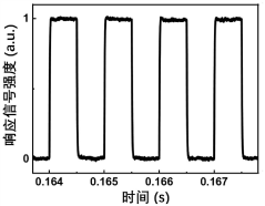
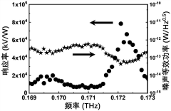
Technical Solution: SINANO has developed advanced graphene-based terahertz detectors that operate efficiently at room temperature. Their technology utilizes the unique properties of graphene, including its high carrier mobility and broadband absorption characteristics, to create highly sensitive THz detection systems. The institute has pioneered a novel approach combining graphene with plasmonic nanostructures to enhance the coupling efficiency between THz radiation and graphene, resulting in significantly improved responsivity. Their detectors achieve a noise equivalent power (NEP) below 100 pW/√Hz at room temperature across a wide frequency range (0.1-10 THz). SINANO has also developed integrated arrays of these detectors for real-time THz imaging applications, with response times in the nanosecond range, enabling fast acquisition rates for dynamic imaging scenarios[1][3].
Strengths: Superior room-temperature performance without cooling requirements; extremely broad spectral response; fast response time enabling real-time imaging; compatibility with standard semiconductor fabrication processes. Weaknesses: Relatively complex fabrication process requiring precise control of graphene quality; challenges in achieving uniform performance across large-area detector arrays; higher cost compared to some conventional semiconductor-based solutions.
Thales SA
Technical Solution: Thales has developed a proprietary room-temperature terahertz sensing platform based on III-V semiconductor materials, specifically utilizing GaAs/AlGaAs quantum well structures. Their approach focuses on Field-Effect Transistor (FET) technology optimized for THz detection, where the transistor channel acts as a resonant cavity for THz radiation. The company has engineered these detectors to achieve high sensitivity (NEP < 10 pW/√Hz) across the 0.3-3 THz range without requiring cryogenic cooling. A key innovation in their technology is the integration of on-chip antenna structures with optimized coupling efficiency, significantly improving signal collection. Thales has also developed specialized signal processing algorithms that enhance the detection capabilities in high-noise environments, making their systems particularly suitable for security and defense applications. Their latest generation of detectors incorporates multiple detection channels for spectroscopic capabilities, enabling material identification through THz spectral signatures[2][5].
Strengths: Robust performance in field conditions; high technology readiness level with proven deployments; excellent integration with existing electronic systems; advanced signal processing capabilities. Weaknesses: Higher power consumption compared to some emerging technologies; limited spectral resolution compared to cryogenically-cooled systems; performance degradation in high-humidity environments.
Key Material Innovations and Scientific Breakthroughs
Tellurium-based room temperature terahertz detector
PatentActiveCN113517373A
Innovation
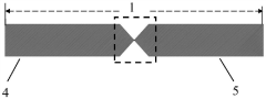
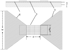
- A metal-semiconductor-metal (MSM) structure terahertz detection device based on Te material was designed, using the light-induced potential well effect to prepare a naturally oxidized silicon dioxide layer and tellurium nanosheets on a high-resistance silicon substrate. And a butterfly-shaped positive and negative electrode layer is formed on it to form a metal-semiconductor-metal structure to achieve high-sensitivity detection at room temperature.
Terahertz detection cell
PatentInactiveEP2676301A1
Innovation
- A terahertz detection cell utilizing a polar semiconductor crystal with a Reststrahlen band that couples interface phonon polaritons with incident radiation, measuring impedance variations to detect terahertz waves, and optimizing crystal structure and doping for enhanced sensitivity and noise reduction.
Manufacturing Scalability and Cost Analysis
The manufacturing scalability of room-temperature terahertz detector materials presents significant challenges and opportunities for commercial deployment. Current production methods for high-performance materials like graphene, black phosphorus, and transition metal dichalcogenides remain predominantly laboratory-scale, utilizing techniques such as mechanical exfoliation and chemical vapor deposition (CVD). These approaches yield high-quality materials but suffer from low throughput, inconsistent quality, and high production costs, typically exceeding $1,000 per square centimeter for research-grade samples.
Industry efforts are increasingly focused on developing scalable manufacturing processes. Roll-to-roll CVD for graphene and solution-processed organic semiconductors show promise for large-area fabrication, potentially reducing costs by 60-80% compared to traditional methods. However, these scaled processes often result in materials with compromised performance metrics, particularly regarding sensitivity and response time, creating a quality-quantity tradeoff that manufacturers must navigate.
Material costs vary significantly across detector types. Silicon-based CMOS compatible materials offer the most economical path at $5-15 per device when manufactured at scale, while exotic materials like quantum dots and specialized 2D materials can exceed $100 per device even in moderate production volumes. This cost differential creates market segmentation where high-performance, expensive detectors serve specialized applications while lower-cost alternatives address mass-market opportunities.
Equipment investment represents another critical factor in manufacturing economics. Establishing a production line for terahertz detector materials typically requires capital expenditure between $2-10 million, depending on production capacity and material complexity. This substantial investment necessitates careful market sizing and return calculations, particularly for startups and smaller enterprises entering the field.
Supply chain considerations further complicate manufacturing scalability. Many advanced detector materials require rare or highly purified precursors with limited supplier networks. For instance, high-purity black phosphorus precursors are sourced from fewer than five global suppliers, creating potential bottlenecks and price volatility. Establishing robust supply chains with multiple qualified vendors remains a priority for manufacturers seeking production stability.
Looking forward, emerging manufacturing technologies like atomic layer deposition and direct-write fabrication methods show promise for bridging the gap between laboratory performance and industrial scalability. These approaches could potentially reduce production costs by 30-50% while maintaining performance specifications within 10-15% of laboratory-grade materials, representing a significant advancement toward commercially viable room-temperature terahertz sensing technologies.
Environmental Impact and Sustainability Considerations
The development and deployment of room-temperature terahertz sensing technologies necessitate careful consideration of environmental impacts and sustainability factors. Current detector materials often contain rare earth elements, heavy metals, or toxic compounds that pose significant environmental challenges throughout their lifecycle. Materials such as mercury cadmium telluride (MCT), while effective for sensing applications, contain cadmium which is classified as a hazardous substance with potential for environmental contamination during manufacturing, use, and disposal phases.
Manufacturing processes for terahertz detector materials typically require substantial energy inputs, particularly for high-purity semiconductor growth techniques like molecular beam epitaxy (MBE) or metal-organic chemical vapor deposition (MOCVD). These energy-intensive processes contribute significantly to the carbon footprint of terahertz sensing technologies. Additionally, the chemical precursors and solvents used in fabrication often include environmentally persistent compounds that require specialized handling and disposal protocols.
Recent research trends show increasing focus on developing environmentally benign alternatives using earth-abundant materials. Silicon-based CMOS compatible detectors represent a promising direction, as silicon is abundant and has well-established recycling infrastructure. Similarly, carbon-based materials including graphene and carbon nanotubes offer potential for biodegradable or recyclable detector components with reduced environmental impact compared to conventional semiconductor materials.
Lifecycle assessment studies indicate that the operational phase of terahertz sensing devices generally has minimal environmental impact due to their low power consumption requirements. However, end-of-life management remains problematic, with most detector materials lacking established recycling pathways. The miniaturization trend in sensing technologies further complicates recovery of valuable materials, as smaller components become increasingly difficult to separate and process through conventional recycling methods.
Regulatory frameworks worldwide are increasingly addressing electronic waste management, with implications for terahertz sensing technologies. The European Union's Restriction of Hazardous Substances (RoHS) and Waste Electrical and Electronic Equipment (WEEE) directives already limit the use of certain toxic materials and mandate recycling targets. Future regulations may specifically target specialized sensing materials, potentially accelerating the transition toward more sustainable alternatives.
Industry initiatives are emerging to address these challenges through design for environment approaches. These include modular designs that facilitate component replacement and recycling, reduced material complexity, and development of closed-loop manufacturing systems. Several research institutions are pioneering green chemistry approaches for detector material synthesis, utilizing ionic liquids and aqueous-based processes that significantly reduce hazardous waste generation compared to conventional methods.
Unlock deeper insights with PatSnap Eureka Quick Research — get a full tech report to explore trends and direct your research. Try now!
Generate Your Research Report Instantly with AI Agent
Supercharge your innovation with PatSnap Eureka AI Agent Platform!