THz Waveguide And Lens Designs For Industrial Imaging Heads
AUG 29, 202510 MIN READ
Generate Your Research Report Instantly with AI Agent
Patsnap Eureka helps you evaluate technical feasibility & market potential.
THz Imaging Technology Background and Objectives
Terahertz (THz) imaging technology has emerged as a revolutionary approach in non-destructive testing and industrial inspection over the past three decades. Operating in the frequency range between 0.1 and 10 THz, this technology bridges the gap between microwave and infrared regions of the electromagnetic spectrum, offering unique capabilities that neither conventional optical nor X-ray imaging can provide. The historical development of THz imaging can be traced back to the early 1990s, when the first THz time-domain spectroscopy systems were demonstrated, followed by imaging applications in the late 1990s.
The evolution of THz technology has been marked by significant breakthroughs in source and detector technologies, transitioning from bulky, expensive laboratory setups to more compact, cost-effective systems suitable for industrial deployment. Recent advancements in quantum cascade lasers, photoconductive antennas, and solid-state electronic sources have dramatically improved the power, efficiency, and reliability of THz systems, making industrial applications increasingly viable.
Waveguides and lens designs represent critical components in THz imaging systems, particularly for industrial imaging heads where precision, robustness, and integration capabilities are paramount. Traditional approaches have relied on free-space propagation and conventional optics, which often suffer from high losses, limited focusing capabilities, and integration challenges in industrial environments. The development of specialized THz waveguides and lens designs aims to overcome these limitations, enabling more efficient energy delivery and improved spatial resolution.
The primary technical objectives for THz waveguide and lens designs in industrial imaging heads include: reducing transmission losses to maximize signal-to-noise ratio; enhancing spatial resolution to detect smaller defects; improving beam quality and control for consistent imaging performance; minimizing system size and complexity for practical industrial integration; and ensuring compatibility with harsh industrial environments including temperature variations, vibrations, and dust.
Additionally, there is a growing emphasis on developing multi-functional imaging heads capable of simultaneous multi-spectral analysis, which requires innovative waveguide and lens designs that can efficiently handle multiple frequency bands. The ultimate goal is to create industrial THz imaging systems that offer real-time, high-resolution capabilities comparable to optical systems but with the penetration advantages of THz radiation.
Current research trends are focusing on metamaterial-based lenses, photonic crystal waveguides, and 3D-printed THz components that promise to revolutionize the field by offering unprecedented control over THz wave propagation and focusing. These developments align with the broader industrial trend toward more intelligent, automated inspection systems that can provide comprehensive material characterization beyond simple imaging.
Industrial Market Demand for THz Imaging Solutions
The industrial market for THz imaging solutions has witnessed significant growth in recent years, driven by the increasing demand for non-destructive testing and quality control across various manufacturing sectors. THz imaging offers unique advantages over traditional inspection methods, including the ability to penetrate non-metallic materials, detect hidden defects, and provide high-resolution images without harmful radiation.
Manufacturing industries, particularly electronics, automotive, and aerospace, represent the largest market segments for THz imaging technologies. In electronics manufacturing, THz imaging enables the inspection of semiconductor packages, printed circuit boards, and integrated circuits for defects that are invisible to conventional optical inspection systems. The semiconductor industry's continuous miniaturization trend has created a growing need for more precise inspection tools capable of detecting microscopic flaws.
The automotive sector has embraced THz imaging for quality control in composite materials, adhesive bonds, and paint thickness measurements. As vehicles incorporate more lightweight materials and complex assemblies, the demand for non-destructive testing solutions that can verify structural integrity without compromising the components has increased substantially.
Pharmaceutical manufacturing represents another significant market opportunity, where THz imaging facilitates tablet coating inspection, package seal integrity verification, and chemical composition analysis. Regulatory requirements for pharmaceutical quality control have become more stringent, driving adoption of advanced inspection technologies that can ensure product safety and efficacy.
Food processing industries have also shown interest in THz imaging for foreign object detection and quality assessment, particularly as consumers demand higher quality standards and regulatory bodies enforce stricter safety protocols. The ability to detect contaminants through packaging without opening products offers significant value to food manufacturers.
Market research indicates that the global THz imaging market is projected to grow at a compound annual growth rate exceeding 20% through 2028, with industrial applications accounting for approximately half of this market. North America currently leads in adoption, followed by Europe and Asia-Pacific, though the latter is experiencing the fastest growth rate due to rapid industrialization.
Key market drivers include increasing quality control requirements, growing automation in manufacturing processes, and the need for more sophisticated non-destructive testing methods. However, market penetration faces challenges related to system cost, technical expertise requirements, and integration complexities with existing production lines. As waveguide and lens designs improve to create more compact, efficient, and cost-effective THz imaging heads, these barriers are expected to diminish, accelerating market adoption across diverse industrial sectors.
Current THz Waveguide and Lens Technical Challenges
The terahertz (THz) frequency range, spanning from 0.1 to 10 THz, offers unique advantages for industrial imaging applications due to its non-ionizing nature and ability to penetrate non-metallic materials. However, the development of effective waveguide and lens systems for THz industrial imaging heads faces significant technical challenges that currently limit widespread adoption.
Material limitations represent one of the most fundamental obstacles in THz waveguide and lens design. Conventional optical materials exhibit prohibitively high absorption in the THz range, while traditional microwave waveguide materials struggle with dimensional precision at these frequencies. High-resistivity silicon and specialized polymers like TOPAS and Zeonex show promise but remain expensive and difficult to process with the required precision.
Propagation losses in THz waveguides present another critical challenge. The wavelength-dependent absorption and scattering mechanisms in this frequency range result in substantial signal attenuation over relatively short distances. Current hollow metallic waveguides and dielectric-lined structures achieve losses of approximately 1-5 dB/m, which remains insufficient for many industrial applications requiring longer transmission paths.
Dimensional constraints pose significant engineering difficulties. The THz wavelength range (30μm to 3mm) necessitates waveguide and lens structures with extremely precise dimensions and surface quality. Manufacturing tolerances must typically be maintained below λ/10, requiring nanometer-scale precision for higher frequencies. Current fabrication technologies struggle to consistently achieve these specifications at reasonable costs.
Coupling efficiency between different components in THz systems remains suboptimal. The modal mismatch between free-space propagating THz beams and waveguide modes can result in coupling losses exceeding 3dB per junction. This significantly impacts the overall system performance, particularly in multi-component industrial imaging heads where signal strength is critical.
Dispersion effects in THz waveguides distort pulse shapes and limit bandwidth, creating challenges for broadband imaging applications. Current waveguide designs exhibit group velocity dispersion that restricts effective bandwidths to approximately 20-30% of the center frequency, limiting imaging resolution and depth information.
Environmental sensitivity further complicates THz waveguide and lens implementation. Water vapor absorption lines throughout the THz spectrum create atmospheric windows that constrain operational frequencies. Additionally, temperature fluctuations in industrial environments can alter the refractive properties of THz optical materials, necessitating complex compensation mechanisms that add cost and complexity.
Integration challenges with existing industrial systems represent another significant hurdle. THz components typically require specialized interfaces and precise alignment tolerances that are difficult to maintain in vibration-prone industrial environments. Current solutions often involve bulky mechanical structures that limit deployment flexibility.
Current Waveguide and Lens Design Approaches
01 THz waveguide structures and materials
Various waveguide structures are designed specifically for THz frequency applications, including hollow-core, parallel-plate, and dielectric waveguides. These structures utilize specialized materials and geometries to minimize signal loss and dispersion while maximizing transmission efficiency in the terahertz range. Advanced materials such as low-loss polymers, semiconductors, and metamaterials are employed to enhance waveguide performance and enable effective THz wave propagation over practical distances.- THz waveguide structures and materials: Various waveguide structures and materials are utilized for efficient THz wave transmission. These include hollow-core waveguides, dielectric waveguides, and metamaterial-based waveguides that can minimize losses and dispersion in the THz frequency range. The design of these waveguides often incorporates specialized geometries and material combinations to enhance transmission efficiency and bandwidth while reducing signal attenuation.
- THz lens design and focusing techniques: THz lens designs employ various materials and geometries to effectively focus and manipulate THz radiation. These include diffractive, refractive, and hybrid lens systems optimized for the THz spectrum. Advanced lens designs incorporate novel materials with appropriate refractive indices and low absorption in the THz range, along with specialized surface profiles to minimize aberrations and maximize focusing efficiency for imaging and sensing applications.
- Integration of THz components in communication systems: THz waveguides and lenses are integrated into communication systems to enable high-bandwidth data transmission. These components are designed to efficiently couple, route, and focus THz radiation within communication devices. The integration involves specialized coupling mechanisms between waveguides and antennas, compact packaging solutions, and alignment techniques to maintain signal integrity throughout the system while minimizing losses at interfaces between components.
- Novel fabrication methods for THz optical components: Advanced fabrication techniques are employed to create precise THz waveguides and lenses. These methods include micromachining, 3D printing, semiconductor processing, and nanofabrication approaches specifically adapted for THz components. The fabrication processes are optimized to achieve the required dimensional accuracy, surface quality, and material properties necessary for efficient THz wave manipulation while enabling cost-effective manufacturing of complex geometries.
- THz sensing and imaging applications: Specialized waveguide and lens designs are developed for THz sensing and imaging applications. These components enable high-resolution imaging, spectroscopy, and detection systems operating in the THz range. The designs focus on maximizing signal collection efficiency, improving spatial resolution, and enhancing sensitivity for applications in security screening, non-destructive testing, biomedical imaging, and quality control in manufacturing processes.
02 THz lens design and focusing techniques
Specialized lens designs for THz applications focus on optimizing beam shaping and focusing capabilities. These include diffractive, Fresnel, hyperbolic, and metamaterial-based lenses that overcome traditional limitations in the terahertz range. Advanced manufacturing techniques enable the creation of precise lens geometries with features optimized for specific THz wavelengths, resulting in improved focusing efficiency, reduced aberrations, and enhanced spatial resolution for imaging and sensing applications.Expand Specific Solutions03 Integrated THz waveguide-lens systems
Integrated systems combining waveguide and lens technologies create compact, efficient THz components for communications and sensing. These designs feature seamless transitions between waveguide structures and focusing elements to minimize coupling losses and maximize signal integrity. Integration approaches include monolithic fabrication of waveguide-lens assemblies, hybrid integration of discrete components, and novel coupling mechanisms that efficiently transfer THz radiation between guided-wave and free-space propagation regimes.Expand Specific Solutions04 THz waveguide and lens fabrication methods
Advanced fabrication techniques for THz components include micromachining, 3D printing, semiconductor processing, and precision molding. These methods enable the creation of complex geometries with feature sizes appropriate for THz wavelengths while maintaining tight tolerances. Material selection and processing parameters are optimized to minimize absorption losses and surface roughness, which are critical factors affecting the performance of THz waveguides and lenses.Expand Specific Solutions05 Novel applications of THz waveguides and lenses
THz waveguides and lenses enable emerging applications in communications, sensing, imaging, and spectroscopy. These include high-bandwidth wireless data transmission, non-destructive testing, security screening, medical diagnostics, and material characterization. Specialized designs address application-specific requirements such as beam steering for communications, high resolution for imaging, or specific frequency selectivity for spectroscopic applications, demonstrating the versatility of THz waveguide and lens technologies across multiple fields.Expand Specific Solutions
Key Industrial Players in THz Imaging Systems
THz waveguide and lens designs for industrial imaging heads are currently in an emerging growth phase, with the market expanding as industrial applications increasingly adopt terahertz technology. The global market size is projected to reach significant scale as manufacturing sectors recognize the non-destructive testing capabilities of THz imaging. Technologically, the field shows varying maturity levels across players. Academic institutions like Tianjin University, Rice University, and Peking University are advancing fundamental research, while companies including BOE Technology, Corning, and IMRA America are developing commercial applications. Research organizations such as Electronics & Telecommunications Research Institute and Shanghai Institute of Optics & Fine Mechanics are bridging theoretical concepts with practical implementations. The competitive landscape features collaboration between academia and industry, with specialized companies like Tetechs and DigiLens focusing on innovative waveguide designs for industrial deployment.
William Marsh Rice University
Technical Solution: Rice University has developed pioneering THz waveguide and lens technologies through their renowned photonics and nanophotonics research groups. Their waveguide approach centers on subwavelength plasmonic structures that enable tight confinement and manipulation of THz radiation with dimensions significantly smaller than conventional waveguides. These plasmonic waveguides utilize precisely engineered metal-dielectric interfaces to support surface plasmon polaritons at THz frequencies, achieving propagation losses significantly lower than traditional metallic waveguides. For industrial imaging applications, Rice has developed novel hyperbolic metamaterial lenses that overcome the diffraction limit through careful engineering of electromagnetic anisotropy. These flat lenses achieve super-resolution imaging capabilities by manipulating the dispersion of THz waves through nanoscale structured surfaces. Their integrated imaging head designs incorporate both waveguide and lens technologies with innovative coupling mechanisms that maximize energy transfer between components. Rice's solutions also feature adaptive beam control through reconfigurable metamaterial elements, allowing dynamic adjustment of imaging parameters without mechanical movement, which is particularly valuable for automated industrial inspection systems requiring variable resolution or field-of-view.
Strengths: Cutting-edge research producing novel approaches beyond conventional technology; strong theoretical foundation enabling fundamental performance advantages; interdisciplinary expertise spanning electromagnetics, materials science, and fabrication techniques. Weaknesses: Academic origin may present challenges in manufacturing scalability; advanced technologies might require specialized fabrication capabilities limiting mass production; solutions may prioritize performance demonstrations over industrial practicality and cost-effectiveness.
Corning, Inc.
Technical Solution: Corning has developed advanced THz waveguide solutions utilizing their expertise in specialty glass and ceramic materials. Their technology incorporates low-loss dielectric waveguides specifically designed for industrial imaging applications in the terahertz frequency range (0.1-10 THz). The company's proprietary waveguide designs feature hollow-core structures with specialized internal coatings that minimize signal attenuation while maintaining beam quality across distances required for industrial scanning. Complementing their waveguides, Corning has engineered gradient-index (GRIN) THz lenses that offer superior focusing capabilities with minimal chromatic aberration across broad THz bandwidths. These components are manufactured using precision molding techniques that ensure consistent optical performance while enabling cost-effective mass production for industrial deployment. Corning's integrated THz imaging heads combine their waveguide and lens technologies with custom coupling mechanisms to efficiently interface with both continuous-wave and pulsed THz sources.
Strengths: Exceptional material expertise allows for low-loss THz transmission; established manufacturing infrastructure enables consistent quality and scalability; integrated solutions approach simplifies system integration. Weaknesses: Higher production costs compared to conventional optical components; limited flexibility for customization in rapidly evolving application spaces; performance may be optimized for specific frequency bands rather than full THz spectrum.
Critical Patents in THz Imaging Head Design
Terahertz tunable sources, spectrometers, and imaging systems
PatentInactiveUS8035083B1
Innovation
- A combination of a low-frequency backward wave oscillator (BWO) coupled with a single-mode waveguide and a Schottky-diode-based frequency multiplier, enabling tunable terahertz generation with enhanced output power and spectral range from 0.1 THz to 1 THz, using a compact and lightweight design that suppresses residual radiation and optimizes power coupling.
Nonlinear crystal and waveguide array for generation of terahertz radiation
PatentInactiveUS7787724B2
Innovation
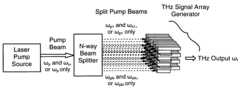
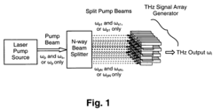
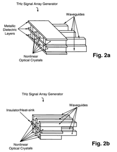
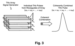
- A system utilizing an array of nonlinear optical crystals coupled with waveguides, where each crystal receives a pump beam to generate terahertz signals, which are then coherently combined to produce high-power terahertz radiation, employing techniques like difference frequency mixing and optical parametric oscillation, with materials such as zinc germanium phosphide and gallium arsenide, and using metallic dielectric layers for modal dispersion control.
Materials Science Advancements for THz Components
Recent advancements in materials science have significantly propelled the development of terahertz (THz) components, particularly for waveguides and lenses used in industrial imaging heads. Traditional materials like silicon and quartz have been supplemented by innovative composites and metamaterials that offer superior performance characteristics in the THz frequency range (0.1-10 THz).
Polymer-based materials have emerged as promising candidates for THz components due to their low absorption coefficients and favorable dielectric properties. Specifically, cyclic olefin copolymers (COC) and cyclic olefin polymers (COP) demonstrate exceptional transparency in the THz range while offering manufacturing advantages through injection molding and 3D printing techniques. These materials enable the production of complex lens geometries that were previously difficult to achieve with conventional materials.
Metamaterials engineered with sub-wavelength structures have revolutionized THz component design by enabling precise control over electromagnetic wave propagation. These artificially structured materials exhibit properties not found in nature, such as negative refractive indices and near-zero permittivity, which can be leveraged to create super-resolution lenses and highly efficient waveguides. Recent research has demonstrated metamaterial-based THz lenses with focal lengths that can be dynamically adjusted through external stimuli.
Ceramic composites, particularly those incorporating aluminum oxide and zirconium oxide, have shown excellent thermal stability and mechanical durability for industrial THz imaging applications. These materials maintain consistent optical properties across wide temperature ranges, making them suitable for harsh industrial environments where thermal fluctuations could otherwise compromise imaging performance.
Two-dimensional materials like graphene have opened new possibilities for THz components due to their unique electronic properties. Graphene-based waveguides can support surface plasmon polaritons in the THz range, enabling highly confined wave propagation with minimal losses. Furthermore, graphene's conductivity can be tuned through electrical gating, allowing for the development of reconfigurable THz components that adapt to varying imaging requirements.
High-resistivity silicon remains relevant due to advancements in microfabrication techniques that enable the creation of silicon-based photonic crystal structures. These structures can guide and manipulate THz waves with unprecedented precision, while benefiting from compatibility with established semiconductor manufacturing processes. Recent innovations include anti-reflection structured surfaces that significantly reduce reflection losses at material interfaces.
The integration of phase-change materials into THz components represents another frontier, allowing for components that can switch between different optical states. Materials like vanadium dioxide (VO₂) exhibit dramatic changes in their THz optical properties in response to temperature changes or electrical stimulation, enabling the development of tunable filters and switchable waveguides for adaptive imaging systems.
Integration Strategies with Industrial Control Systems
The integration of THz waveguide and lens systems with industrial control infrastructure represents a critical aspect of deploying advanced imaging technology in manufacturing environments. Successful implementation requires seamless communication between the THz imaging heads and existing industrial control systems (ICS) to enable real-time data acquisition, processing, and decision-making capabilities.
Industrial control systems typically operate on standardized protocols such as PROFINET, EtherCAT, or OPC UA, which must interface effectively with the high-bandwidth data streams generated by THz imaging systems. A modular integration approach utilizing middleware solutions can bridge this gap, allowing THz imaging data to be translated into formats compatible with programmable logic controllers (PLCs) and distributed control systems (DCS).
Hardware integration considerations include the development of ruggedized interface modules capable of withstanding harsh industrial environments while maintaining signal integrity. These modules must incorporate appropriate electrical isolation, electromagnetic interference (EMI) shielding, and thermal management to ensure reliable operation alongside conventional industrial equipment.
Software integration frameworks must address several key challenges, including data synchronization between the high-speed THz acquisition systems and relatively slower industrial control loops. Time-stamping mechanisms and buffer management strategies are essential for maintaining temporal coherence between imaging data and process variables. Additionally, edge computing architectures can be deployed to perform preliminary image processing and feature extraction before transmitting reduced data sets to the central control system.
Real-time performance requirements necessitate optimization of data flows between THz imaging heads and control systems. Techniques such as selective data transmission, region-of-interest processing, and adaptive sampling rates can significantly reduce bandwidth requirements while maintaining critical imaging capabilities. Implementation of deterministic networking technologies like Time-Sensitive Networking (TSN) can further enhance system responsiveness.
Security considerations must not be overlooked when integrating advanced imaging systems with industrial controls. Proper network segmentation, encrypted communications, and access control mechanisms should be implemented to protect both the imaging system and the broader industrial network from potential cyber threats. This is particularly important as THz imaging systems may provide insights into proprietary manufacturing processes.
Standardization efforts are emerging to facilitate smoother integration of advanced sensing technologies with industrial control systems. Organizations such as the OPC Foundation and various industry consortia are developing specifications for sensor integration that could be adapted for THz imaging applications, potentially reducing implementation complexity and improving interoperability across different manufacturing environments.
Unlock deeper insights with Patsnap Eureka Quick Research — get a full tech report to explore trends and direct your research. Try now!
Generate Your Research Report Instantly with AI Agent
Supercharge your innovation with Patsnap Eureka AI Agent Platform!