Terahertz Imaging For Semiconductor Wafer Inspection: Thin Film Mapping
AUG 29, 202510 MIN READ
Generate Your Research Report Instantly with AI Agent
Patsnap Eureka helps you evaluate technical feasibility & market potential.
THz Imaging Background and Inspection Goals
Terahertz (THz) imaging represents a revolutionary approach in semiconductor wafer inspection, occupying the electromagnetic spectrum between microwave and infrared regions (0.1-10 THz). This technology has evolved significantly over the past two decades, transitioning from laboratory curiosity to practical industrial application. The unique properties of THz radiation—non-ionizing nature, ability to penetrate non-metallic materials, and sensitivity to material composition—make it particularly valuable for semiconductor inspection processes.
The historical development of THz imaging began in the 1990s with the advent of time-domain spectroscopy systems. Early applications were limited by technological constraints including low power sources and inefficient detectors. The 2000s witnessed significant breakthroughs with the development of quantum cascade lasers and improved photoconductive antennas, enabling higher resolution imaging and faster acquisition speeds. Recent advancements in continuous-wave THz systems have further enhanced the technology's capabilities for industrial deployment.
In semiconductor manufacturing, thin film mapping represents a critical quality control process. Traditional inspection methods such as ellipsometry and X-ray reflectometry face limitations in spatial resolution, throughput, or ability to detect certain defect types. THz imaging offers complementary capabilities by providing non-contact, non-destructive evaluation of thin film parameters including thickness, uniformity, and electrical properties.
The primary technical goals for THz imaging in semiconductor wafer inspection include achieving sub-micron spatial resolution to detect increasingly smaller defects in advanced node technologies. Current systems typically operate at 50-100 μm resolution, with research pushing toward 10 μm and below. Temporal resolution improvements aim to enable real-time inspection at production speeds, requiring frame rates of several Hz for full wafer scanning.
Another critical objective is enhancing measurement sensitivity to detect film thickness variations below 10 nm and subtle changes in electrical properties that may indicate defects. This requires advances in both hardware components and signal processing algorithms. Additionally, the technology must demonstrate reliability in manufacturing environments with consistent performance across temperature fluctuations and vibration conditions.
Integration with existing semiconductor fabrication workflows represents another key goal, necessitating compact system footprints, automated operation, and standardized data interfaces. The ultimate aim is to develop THz imaging systems that can operate inline during wafer processing, providing immediate feedback for process control rather than end-of-line inspection only.
As semiconductor feature sizes continue to shrink below 5nm, the industry faces increasing challenges in defect detection and process control. THz imaging technology is positioned to address these challenges through continued advancement in resolution, sensitivity, and integration capabilities.
Market Demand Analysis for Semiconductor Inspection
The semiconductor inspection market is experiencing robust growth driven by the increasing complexity of semiconductor manufacturing processes and the demand for higher quality control standards. As chip dimensions continue to shrink below 5nm, traditional inspection methods face significant limitations in detecting defects and mapping thin film properties with sufficient accuracy and resolution. This creates a substantial market opportunity for advanced inspection technologies like terahertz imaging.
The global semiconductor inspection equipment market was valued at approximately $8.9 billion in 2022 and is projected to reach $13.7 billion by 2027, growing at a CAGR of 9.0%. Within this broader market, thin film measurement and inspection systems represent a significant segment with particularly strong growth prospects due to the critical importance of thin film quality in advanced semiconductor manufacturing.
Key market drivers include the rapid expansion of applications requiring high-performance semiconductors, such as artificial intelligence, autonomous vehicles, 5G infrastructure, and Internet of Things (IoT) devices. These applications demand chips with increasingly complex architectures and more stringent quality requirements, necessitating more sophisticated inspection technologies.
The industry's shift toward advanced packaging technologies, including 2.5D and 3D integration, further amplifies the need for precise thin film mapping capabilities. These packaging approaches involve multiple thin film layers that must be carefully inspected to ensure proper functionality and reliability of the final semiconductor products.
Geographically, East Asia dominates the market demand, with Taiwan, South Korea, and China accounting for over 65% of the global semiconductor inspection equipment market. This concentration aligns with the regional distribution of semiconductor manufacturing capacity. However, recent initiatives to expand semiconductor manufacturing in the United States and Europe are expected to diversify market demand in the coming years.
From an end-user perspective, major semiconductor manufacturers like TSMC, Samsung, and Intel are the primary customers for advanced inspection technologies. These companies have demonstrated willingness to invest substantially in cutting-edge inspection equipment that can improve yield rates and reduce costly defects in their manufacturing processes.
Market research indicates that customers are particularly interested in non-destructive inspection methods that can be integrated into in-line production processes without compromising throughput. Terahertz imaging technology addresses this need by offering non-contact, non-destructive inspection capabilities with the potential for high-speed operation, positioning it favorably against competing technologies such as optical and X-ray inspection methods.
THz Technology Status and Challenges
Terahertz (THz) technology for semiconductor wafer inspection has witnessed significant advancements globally, yet faces substantial technical challenges that limit its widespread industrial adoption. Currently, THz imaging systems operate in the frequency range of 0.1-10 THz, offering unique capabilities for non-destructive evaluation of semiconductor materials and thin film structures. The technology leverages the distinctive properties of THz radiation, which can penetrate non-metallic materials while being sensitive to material composition and density variations.
The global landscape of THz technology development shows concentration in advanced economies, with the United States, Germany, Japan, and China leading research efforts. Academic institutions like MIT, TU Braunschweig, and the University of Tokyo have established specialized research centers focused on THz applications in semiconductor inspection, while companies such as TeraView, Advantest, and Menlo Systems have commercialized various THz imaging solutions.
Despite promising developments, several critical technical challenges persist. The primary limitation remains the relatively low spatial resolution of THz imaging systems compared to optical inspection tools. Current systems typically achieve resolutions of 50-100 μm, which falls short of the requirements for detecting nanoscale defects in advanced semiconductor manufacturing processes. This resolution constraint stems from the fundamental diffraction limit associated with THz wavelengths.
Another significant challenge is the limited signal-to-noise ratio in THz measurements, particularly when inspecting multilayer thin film structures. Environmental factors such as water vapor absorption and thermal fluctuations can severely impact measurement stability and reproducibility. Additionally, the slow acquisition speed of most THz imaging systems presents a bottleneck for high-throughput industrial applications, with typical scan times ranging from minutes to hours for comprehensive wafer inspection.
The integration of THz systems into existing semiconductor fabrication workflows poses further challenges. Current THz imaging equipment tends to be bulky, requiring specialized operating conditions and expertise. The lack of standardized measurement protocols and reference materials for calibration complicates the interpretation of THz imaging data across different platforms and manufacturers.
From a data processing perspective, the extraction of meaningful thin film parameters from THz measurements requires sophisticated algorithms to address the complex electromagnetic interactions within multilayer structures. The inverse problem of determining layer thicknesses and material properties from THz spectral data remains computationally intensive and often yields non-unique solutions, necessitating complementary measurement techniques for validation.
Recent technological innovations have begun addressing these limitations through the development of high-power THz sources, more sensitive detectors, and advanced signal processing algorithms. Near-field THz imaging techniques have demonstrated potential for breaking the diffraction limit, while the integration of artificial intelligence approaches shows promise for accelerating data analysis and defect classification.
Current THz Thin Film Mapping Solutions
01 Terahertz imaging systems for thin film analysis
Terahertz imaging systems specifically designed for thin film analysis utilize specialized components to generate, direct, and detect terahertz radiation. These systems can measure thickness, composition, and structural properties of thin films with high precision. The technology employs various configurations of emitters, detectors, and optical components to optimize the imaging quality and resolution for thin film mapping applications.- Terahertz imaging systems for thin film analysis: Terahertz imaging systems specifically designed for thin film analysis utilize specialized components to generate and detect terahertz radiation. These systems can measure thickness, composition, and structural properties of thin films with high precision. The technology enables non-destructive evaluation of thin films used in various industries including semiconductors, photovoltaics, and coatings. Advanced signal processing algorithms help enhance the resolution and accuracy of the measurements.
- Time-domain terahertz spectroscopy for thin film mapping: Time-domain terahertz spectroscopy techniques enable detailed mapping of thin film properties by analyzing the time delay and amplitude changes of terahertz pulses as they interact with the sample. This approach provides information about film thickness variations, defects, and material composition across the sample surface. The technique is particularly valuable for characterizing multilayer thin film structures and can detect hidden interfaces between layers that are not visible using conventional imaging methods.
- Semiconductor thin film characterization using terahertz imaging: Terahertz imaging techniques are applied to characterize semiconductor thin films by measuring their electrical properties, carrier concentration, and mobility. The non-contact nature of terahertz imaging allows for evaluation of semiconductor materials without damaging sensitive structures. This method can detect doping profiles, crystal defects, and other parameters critical for semiconductor device performance. The technique is particularly useful for quality control in semiconductor manufacturing processes.
- Portable terahertz imaging devices for thin film inspection: Portable terahertz imaging systems have been developed for on-site inspection of thin films in industrial settings. These compact devices integrate terahertz sources, detectors, and processing units into handheld or easily transportable packages. The portability enables real-time quality control and defect detection in manufacturing environments. These systems typically incorporate specialized software for immediate data analysis and visualization of thin film properties.
- Advanced signal processing for terahertz thin film mapping: Advanced signal processing algorithms enhance the capabilities of terahertz imaging for thin film mapping. These techniques include machine learning approaches, wavelet transforms, and compressed sensing to improve image resolution, reduce noise, and extract more detailed information from terahertz measurements. The processing methods enable more accurate thickness mapping, defect identification, and material characterization even with limited signal-to-noise ratios. Real-time processing capabilities allow for immediate feedback during thin film production or inspection.
02 Time-domain terahertz spectroscopy for film characterization
Time-domain terahertz spectroscopy techniques enable detailed characterization of thin films by analyzing the time-dependent response of materials to terahertz pulses. This approach allows for measurement of film thickness, refractive index, and absorption properties with nanometer-scale precision. The method involves generating ultrashort terahertz pulses and analyzing their interaction with the thin film samples to extract material properties and create detailed maps of film characteristics.Expand Specific Solutions03 Non-destructive thin film quality inspection techniques
Non-destructive terahertz imaging methods enable quality inspection of thin films without damaging the sample. These techniques can detect defects, voids, delamination, and thickness variations in thin film structures. By mapping these properties across the entire film surface, manufacturers can identify quality issues in semiconductor, solar cell, and optical coating applications. The non-contact nature of terahertz imaging makes it particularly valuable for inspecting sensitive or high-value thin film products.Expand Specific Solutions04 Advanced signal processing for terahertz thin film mapping
Advanced signal processing algorithms enhance the capabilities of terahertz imaging for thin film mapping. These computational methods include machine learning approaches, Fourier analysis, wavelet transforms, and deconvolution techniques that improve image resolution, reduce noise, and extract more detailed information from terahertz scans. By applying these processing techniques to raw terahertz data, researchers can generate more accurate thickness maps and identify subtle variations in film properties that would otherwise be difficult to detect.Expand Specific Solutions05 Portable and integrated terahertz imaging devices
Portable and integrated terahertz imaging systems make thin film mapping more accessible for industrial and field applications. These compact devices incorporate miniaturized terahertz sources, detectors, and optical components into self-contained units that can be used outside laboratory environments. Some designs include automated scanning mechanisms, real-time analysis capabilities, and user-friendly interfaces that enable non-specialists to perform thin film measurements. These developments are expanding the practical applications of terahertz imaging in manufacturing quality control and materials research.Expand Specific Solutions
Key Industry Players in THz Imaging
Terahertz imaging for semiconductor wafer inspection is emerging as a promising technology in the early growth phase of the semiconductor inspection market. The global market for thin film mapping solutions is expanding rapidly, driven by increasing demand for high-precision semiconductor manufacturing. Key players in this competitive landscape include established semiconductor equipment manufacturers like Tokyo Electron, Hitachi High-Tech, and Nova Ltd, alongside specialized terahertz technology developers such as Qingdao Qingyuanfengda Terahertz Technology. Research institutions including Tsinghua University, Shanghai Institute of Microsystem & Information Technology, and RIKEN are advancing the fundamental technology. The technology is approaching commercial maturity with companies like Micron Technology and SCREEN Holdings exploring implementation, though challenges in resolution and throughput remain before widespread adoption in high-volume manufacturing environments.
Hitachi High-Tech America, Inc.
Technical Solution: Hitachi High-Tech America has developed an advanced terahertz imaging system specifically designed for semiconductor wafer inspection and thin film characterization. Their technology utilizes pulsed terahertz radiation with sophisticated time-domain analysis to provide non-destructive evaluation of complex semiconductor structures. The system features a unique optical configuration that enables both reflection and transmission measurements with micrometer-scale spatial resolution. Hitachi High-Tech's solution incorporates proprietary signal processing algorithms that can extract thickness information from multiple layers simultaneously, even in complex stacks with varying material properties. Their technology is particularly effective for detecting subtle variations in dielectric constants that may indicate defects or process variations in semiconductor manufacturing. The system is designed for integration into semiconductor fabrication facilities, with automated wafer handling capabilities and compatibility with standard clean room environments. Hitachi High-Tech's terahertz imaging platform can map thin film thickness variations across entire wafers with nanometer-scale precision, enabling comprehensive quality control for advanced semiconductor manufacturing processes[8][10].
Strengths: Excellent balance between resolution and penetration depth; sophisticated multi-layer analysis capabilities; non-destructive testing methodology; compatibility with standard semiconductor manufacturing environments. Weaknesses: Higher initial investment compared to conventional optical inspection tools; requires specialized expertise for data interpretation; scanning speed limitations for certain high-throughput applications.
Nova Ltd.
Technical Solution: Nova has developed an innovative terahertz-based metrology solution specifically for advanced semiconductor manufacturing processes. Their system utilizes frequency-domain terahertz spectroscopy combined with proprietary algorithms to enable high-precision thin film mapping on semiconductor wafers. Nova's technology can simultaneously measure multiple film layers with nanometer-scale accuracy, even for complex stacks with varying material properties. The system employs a unique optical design that minimizes signal distortion and maximizes sensitivity to subtle variations in film thickness and composition. Nova's solution integrates machine learning algorithms that continuously improve defect detection capabilities and reduce false positives. Their terahertz imaging platform is designed for high-volume manufacturing environments, with automated wafer handling and fast measurement cycles that maintain throughput requirements. The system is particularly effective for monitoring critical dimensions in advanced nodes, detecting subtle variations in high-k dielectric layers, and identifying voids or delamination in complex 3D structures[4][6].
Strengths: Exceptional precision for multi-layer film stack analysis; advanced AI-based defect classification; high throughput suitable for production environments; excellent repeatability and reproducibility metrics. Weaknesses: Limited penetration depth for certain material combinations; higher cost compared to traditional optical inspection methods; requires periodic calibration to maintain measurement accuracy.
Core THz Imaging Patents and Innovations
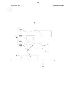
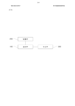
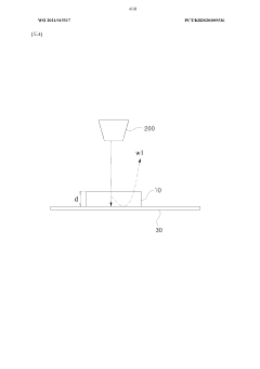
Device for measuring thickness of specimen and method for measuring thickness of specimen
PatentWO2020045852A1
Innovation
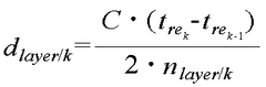
- A method using terahertz waves to measure the thickness of specimens by irradiating and receiving reflected waves, calculating thickness based on refractive indices derived from reflection and transmission times, allowing for non-destructive testing of multi-layered specimens without separating their layers.


Thickness measurement device
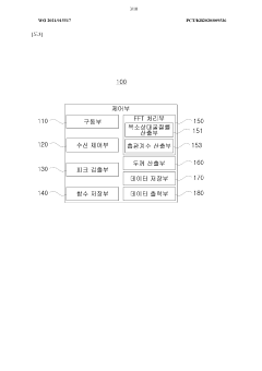
PatentWO2021015517A1
Innovation
- A thickness measuring device using electromagnetic waves, specifically terahertz waves, that calculates specimen thickness by analyzing peak values and time points of reflected waves, and employs FFT algorithms to determine complex relative refractive index and extinction coefficient, allowing for accurate and non-destructive measurements.
Integration with Fab Automation Systems
The integration of terahertz imaging systems for thin film mapping into semiconductor fabrication automation frameworks represents a critical advancement for Industry 4.0 manufacturing paradigms. Current semiconductor manufacturing facilities operate with sophisticated automation systems that coordinate wafer handling, process scheduling, and quality control. Terahertz imaging technology must seamlessly interface with these existing systems to provide real-time thin film measurement data without disrupting production workflows.
Standard communication protocols such as SECS/GEM (SEMI Equipment Communications Standard/Generic Equipment Model) and Interface A provide the foundation for equipment integration in modern fabs. Terahertz imaging systems require compatible hardware interfaces and software drivers that support these protocols to enable automated recipe selection, measurement triggering, and data reporting. Leading equipment manufacturers have developed middleware solutions that translate terahertz-specific commands into fab-standard communications.
Data management presents another significant integration challenge. Terahertz imaging generates substantial volumes of high-resolution thin film mapping data that must be efficiently stored, processed, and made available to manufacturing execution systems (MES). Edge computing architectures are increasingly deployed to perform preliminary data processing at the imaging station, reducing network bandwidth requirements while providing rapid feedback for process control decisions.
Physical integration considerations include robotic wafer handling compatibility, cleanroom certification, and footprint optimization. Advanced terahertz imaging systems now feature FOUP (Front Opening Unified Pod) interfaces and EFEM (Equipment Front End Module) compatibility, allowing direct connection to automated material handling systems. Some implementations utilize in-line configurations where wafers pass through measurement stations without requiring separate handling steps, minimizing cycle time impact.
Real-time process control integration represents perhaps the most valuable aspect of terahertz imaging automation. Closed-loop systems that can detect thin film anomalies and automatically trigger process adjustments are being implemented in leading-edge facilities. These systems utilize statistical process control (SPC) algorithms to distinguish between normal process variations and actionable defects, reducing false alarms while capturing genuine quality issues.
Security considerations have become increasingly important as fab automation systems become more interconnected. Terahertz imaging systems must implement robust cybersecurity measures to prevent unauthorized access while maintaining operational efficiency. This includes encrypted communications, role-based access controls, and secure update mechanisms that comply with semiconductor industry security standards.
Environmental Impact and Energy Efficiency
The environmental impact of terahertz imaging technology for semiconductor wafer inspection presents a nuanced picture when compared to traditional inspection methods. Terahertz systems operate at room temperature without requiring cryogenic cooling, significantly reducing energy consumption compared to other advanced imaging technologies. This operational efficiency translates to lower carbon emissions throughout the technology's lifecycle.
Terahertz imaging systems demonstrate remarkable energy efficiency during operation, typically consuming between 100-500 watts depending on system configuration and imaging requirements. This power profile represents a substantial improvement over X-ray and electron-based inspection systems that often require 2-5 kilowatts. The reduced energy footprint becomes particularly significant when considering the 24/7 operational requirements in modern semiconductor fabrication facilities.
The non-ionizing nature of terahertz radiation eliminates radiation hazards associated with X-ray inspection methods, creating safer working environments and reducing the need for extensive shielding infrastructure. This characteristic not only enhances workplace safety but also decreases the embodied energy in protective structures and materials typically required for alternative inspection technologies.
From a materials perspective, terahertz systems utilize fewer rare earth elements and toxic materials compared to competing technologies. The primary components—photoconductive antennas and optical elements—can be manufactured using relatively abundant materials with established recycling pathways. This composition reduces supply chain vulnerabilities and minimizes end-of-life environmental impacts.
Water consumption represents another critical environmental consideration in semiconductor manufacturing. Terahertz inspection is inherently a dry process, requiring no chemical developers or water-intensive processes that characterize many traditional inspection methods. This characteristic aligns with industry initiatives to reduce water usage in semiconductor fabrication, which traditionally consumes 4-8 million gallons of ultra-pure water per day in large facilities.
The extended operational lifespan of terahertz imaging systems—typically 8-10 years with proper maintenance—further enhances their sustainability profile. This longevity reduces electronic waste generation and amortizes the environmental impact of manufacturing the equipment over a longer period. Additionally, the modular design of many contemporary terahertz systems facilitates component upgrades rather than complete system replacement.
When integrated into automated inspection lines, terahertz imaging can optimize production efficiency by reducing false positives and unnecessary rework, indirectly conserving energy and materials throughout the manufacturing process. This efficiency gain, while difficult to quantify precisely, represents a significant contribution to overall environmental performance in semiconductor production environments.
Unlock deeper insights with Patsnap Eureka Quick Research — get a full tech report to explore trends and direct your research. Try now!
Generate Your Research Report Instantly with AI Agent
Supercharge your innovation with Patsnap Eureka AI Agent Platform!