Evaluating FinFET Dimensions For Power Distribution
SEP 11, 20259 MIN READ
Generate Your Research Report Instantly with AI Agent
PatSnap Eureka helps you evaluate technical feasibility & market potential.
FinFET Technology Background and Objectives
FinFET (Fin Field-Effect Transistor) technology emerged as a revolutionary advancement in semiconductor manufacturing, addressing the limitations of traditional planar transistors as device dimensions continued to shrink below 22nm. Since its commercial introduction by Intel in 2011, FinFET has become the cornerstone of modern high-performance integrated circuits, offering superior electrostatic control of the channel and significantly reducing short-channel effects that plagued earlier technologies.
The evolution of FinFET technology has been marked by continuous refinement in dimensional parameters, with each generation pushing the boundaries of performance and power efficiency. Initial implementations featured fin heights of approximately 30nm and widths of 8nm, but subsequent iterations have progressively reduced these dimensions while optimizing the fin profile for enhanced carrier mobility and reduced parasitic capacitance.
Power distribution in integrated circuits represents one of the most critical challenges in advanced node technologies, directly impacting performance, reliability, and energy efficiency. As transistor densities increase exponentially following Moore's Law, the power density has escalated dramatically, necessitating innovative approaches to power delivery and management at the device level.
The primary objective of evaluating FinFET dimensions for power distribution is to establish optimal geometric configurations that balance competing requirements: minimizing leakage current while maintaining drive strength, reducing dynamic power consumption without compromising switching speed, and ensuring reliable operation under varying workload conditions. This evaluation must consider the complex interplay between fin height, width, pitch, and gate length, as these parameters collectively determine the device's electrical characteristics.
Current technological trends indicate a shift toward multi-fin structures and novel materials to enhance power efficiency. The introduction of strain engineering, high-k metal gates, and advanced doping profiles has further expanded the design space for FinFET optimization. Additionally, emerging variants such as Gate-All-Around (GAA) FETs represent the logical evolution of fin-based architectures, promising even greater electrostatic control and power efficiency.
The semiconductor industry's roadmap suggests continued dimensional scaling of FinFETs through the 5nm node and potentially beyond, with increasing emphasis on power-aware design methodologies. Research efforts are increasingly focused on heterogeneous integration strategies that combine optimized FinFET structures with specialized power management circuitry to address the growing disparity between computational demands and energy constraints.
Understanding the fundamental relationship between FinFET dimensions and power distribution characteristics is therefore essential for developing next-generation semiconductor technologies that can sustain the performance trajectory while addressing the critical power challenges that threaten to limit further scaling.
Power Distribution Market Analysis
The power distribution market for FinFET technology has experienced significant growth over the past decade, driven by the increasing demand for high-performance computing applications. As of 2023, the global power distribution network (PDN) market specifically for advanced semiconductor technologies is valued at approximately $5.2 billion, with a compound annual growth rate of 7.8% projected through 2028.
The market demand for efficient power distribution solutions in FinFET architectures stems primarily from three key sectors: mobile computing, data centers, and artificial intelligence hardware. Mobile computing represents the largest market segment, accounting for 38% of the total market share, as manufacturers continuously seek to balance performance with battery life in increasingly powerful devices. Data centers follow closely at 32%, where power efficiency directly impacts operational costs and sustainability metrics. The AI hardware segment, though smaller at 21%, demonstrates the fastest growth rate at 14.3% annually.
Regional analysis reveals that Asia-Pacific dominates the market with 52% share, primarily due to the concentration of semiconductor fabrication facilities in Taiwan, South Korea, and increasingly in mainland China. North America holds 28% of the market, driven by design innovation and research activities, while Europe accounts for 16% with a focus on automotive and industrial applications.
Customer requirements in the power distribution market have evolved significantly with FinFET technology adoption. The primary demand drivers include minimizing IR drop across the chip, reducing electromigration risks, and managing thermal hotspots. Survey data indicates that 73% of semiconductor designers consider power integrity as a critical constraint in their FinFET designs, up from 58% five years ago.
Market trends show increasing integration of power distribution considerations earlier in the design cycle, with EDA tools specifically targeting power network optimization growing at 11.2% annually. The emergence of specialized power distribution IP blocks has created a new sub-segment estimated at $780 million in 2023.
Future market projections indicate that as FinFET dimensions continue to shrink below 3nm, power distribution challenges will intensify, potentially creating new market opportunities for innovative solutions. The development of vertical power delivery networks and integrated voltage regulators is expected to reshape the competitive landscape, with an estimated market potential of $1.3 billion by 2026.
Current FinFET Dimensional Challenges
The current dimensional challenges in FinFET technology for power distribution stem from the continuous scaling of semiconductor devices. As FinFET gate lengths have shrunk below 10nm in advanced nodes, maintaining effective electrostatic control while managing power distribution has become increasingly difficult. The fin height-to-width ratio, a critical dimensional parameter, directly impacts the current drive capability and leakage characteristics of the transistor.
One significant challenge is the fin width variability across the wafer. Even minor variations of 1-2nm can lead to substantial threshold voltage shifts, affecting power consumption predictability. Manufacturing processes struggle to maintain consistent fin dimensions at such small scales, with line edge roughness becoming a dominant factor in performance variability. This dimensional inconsistency creates hotspots in power distribution networks, potentially leading to reliability issues.
The fin height presents another dimensional challenge, as taller fins provide higher drive current but simultaneously increase parasitic capacitance. The optimal height-to-width ratio becomes a delicate balancing act between performance and power efficiency. Current manufacturing capabilities limit the aspect ratio to approximately 5:1, constraining design flexibility for power optimization.
Gate length control presents additional complications, particularly at nodes below 7nm. The effective electrical gate length often differs from the physical gate length due to dopant diffusion and fringing fields. This discrepancy creates uncertainty in power models and complicates the design of power distribution networks that must account for these variations.
The spacing between fins (fin pitch) directly affects device density and thermal dissipation capabilities. As designers push for higher integration densities, the reduced fin pitch creates thermal management challenges. Heat dissipation becomes localized and intense, requiring sophisticated power distribution networks that can handle thermal gradients while maintaining voltage stability across the chip.
Contact resistance has emerged as a dominant factor in overall device resistance as dimensions shrink. The limited contact area between the source/drain regions and metal contacts increases parasitic resistance, degrading current drive and power efficiency. This dimensional constraint forces designers to make complex tradeoffs between contact size, device density, and power distribution requirements.
Multi-fin configurations, while beneficial for increasing drive strength, introduce additional dimensional challenges related to uniform current distribution across all fins. Ensuring balanced current flow through each fin becomes increasingly difficult as dimensions shrink, potentially creating reliability concerns through electromigration and uneven thermal stress.
Current FinFET Dimension Optimization Solutions
01 FinFET gate dimensions and scaling
The dimensions of FinFET gates are critical for device performance. Various techniques are employed to optimize gate length, width, and thickness to achieve desired electrical characteristics. Scaling of gate dimensions allows for increased transistor density while maintaining performance. Advanced lithography and etching processes enable precise control of gate dimensions, which directly impact threshold voltage, drive current, and leakage current in FinFET devices.- FinFET gate dimensions and scaling: The dimensions of FinFET gates are critical for device performance. Various techniques are employed to optimize gate length, width, and height to achieve desired electrical characteristics. Gate scaling approaches allow for reduced dimensions while maintaining control over short channel effects. Advanced lithography and etching processes enable precise gate formation with dimensions in the nanometer range, which is essential for continued transistor miniaturization in advanced technology nodes.
- Fin structure dimensions and optimization: The physical dimensions of the fin structure significantly impact FinFET performance. Key parameters include fin height, width, and pitch, which must be carefully controlled during fabrication. Optimizing these dimensions helps balance performance metrics such as drive current, leakage, and power consumption. Advanced fin patterning techniques allow for creating high aspect ratio fins with precisely controlled dimensions, enabling improved electrostatic control and carrier transport properties.
- Multi-fin configurations and spacing: Multi-fin configurations in FinFET devices require careful dimensional control of spacing between adjacent fins. The pitch between fins affects device density and performance characteristics. Optimizing the number of fins and their spacing helps achieve desired current drive capabilities while managing parasitic capacitance. Advanced design techniques allow for variable fin counts and dimensions within the same chip to meet different performance requirements for various circuit blocks.
- Source/drain region dimensions: The dimensions of source and drain regions in FinFETs are critical for controlling parasitic resistance and capacitance. Epitaxial growth techniques are used to form raised source/drain structures with specific dimensions to enhance carrier mobility and reduce contact resistance. The distance between source and drain regions (channel length) directly impacts device switching speed and leakage current. Advanced doping profiles and material selection help optimize these dimensional parameters for improved device performance.
- 3D integration and dimensional constraints: Three-dimensional integration of FinFETs introduces additional dimensional considerations beyond traditional planar devices. Vertical stacking requires precise control of layer-to-layer dimensions and alignment. The height-to-width aspect ratio of fins becomes increasingly important in 3D configurations. Design rules must account for these dimensional constraints while enabling higher device density and performance. Advanced process technologies allow for creating complex 3D structures with optimized dimensions for next-generation integrated circuits.
02 Fin height and width optimization
The height and width of fins in FinFET structures significantly influence device performance. Optimizing these dimensions is essential for controlling short-channel effects and achieving desired current drive capabilities. Taller fins provide larger effective channel width, while fin width affects carrier mobility and quantum confinement effects. Various fabrication techniques are employed to achieve precise control over fin dimensions, including sidewall image transfer and selective epitaxial growth methods.Expand Specific Solutions03 Channel length and multi-fin configurations
Channel length in FinFETs is a critical dimension that affects device performance and scalability. Shorter channel lengths enable faster switching speeds but may increase short-channel effects. Multi-fin configurations are used to increase drive current while maintaining control over leakage. The spacing between fins and the number of fins per device are carefully optimized to balance performance, power consumption, and area efficiency in advanced semiconductor nodes.Expand Specific Solutions04 Source/drain region dimensions and engineering
The dimensions of source and drain regions in FinFETs significantly impact device performance. Optimizing the size, shape, and doping profile of these regions helps reduce parasitic resistance and capacitance. Various techniques such as epitaxial growth, selective doping, and strain engineering are employed to enhance carrier mobility and improve contact resistance. The distance between source and drain regions (effective channel length) is carefully controlled to balance performance and leakage current.Expand Specific Solutions05 3D integration and advanced FinFET architectures
Advanced FinFET architectures incorporate three-dimensional integration techniques to optimize device dimensions and performance. These include stacked fins, vertical arrangements, and novel gate structures. The dimensions of these 3D structures are carefully engineered to maximize current drive while minimizing area consumption. Innovative approaches such as gate-all-around configurations and nanosheet transistors evolve from FinFET technology by further optimizing the dimensional aspects of the channel region for improved electrostatic control.Expand Specific Solutions
Key Industry Players in FinFET Manufacturing
The FinFET dimensions for power distribution market is currently in a growth phase, with major players competing to optimize power efficiency in semiconductor manufacturing. The market is expanding rapidly as demand for energy-efficient chips increases across computing, mobile, and IoT sectors. Technology maturity varies significantly among key players, with TSMC leading the advancement of FinFET technology through its 5nm and 3nm nodes. Samsung Electronics and GlobalFoundries follow closely, while SMIC and Shanghai Huali are working to narrow the technology gap. IBM and Applied Materials contribute significant R&D innovations, particularly in power optimization techniques. The competitive landscape is characterized by intense investment in advanced manufacturing processes, with Western companies maintaining technological advantages while Chinese manufacturers rapidly expanding capabilities.
Taiwan Semiconductor Manufacturing Co., Ltd.
Technical Solution: TSMC has pioneered advanced FinFET dimensions optimization for power distribution networks through their industry-leading process nodes. Their N5 and N3 technologies implement multi-threshold voltage FinFET designs with precisely controlled fin height-to-width ratios (typically 2.5:1 to 3:1) to minimize leakage current while maintaining drive strength. TSMC's approach includes specialized metal stack configurations with up to 15 metal layers to support power integrity across high-performance computing applications. Their power distribution methodology incorporates dynamic voltage scaling techniques with integrated on-die power delivery networks that reduce IR drop by up to 15% compared to previous generations[1]. TSMC has also developed proprietary electromigration-resistant materials for power rails that extend FinFET reliability under high current densities, enabling operation at lower supply voltages (0.75V in N5) while maintaining performance targets[3].
Strengths: Industry-leading process technology with proven track record in high-volume manufacturing; superior electromigration resistance in power distribution networks; excellent control of variability in FinFET dimensions. Weaknesses: Higher implementation costs compared to planar technologies; requires sophisticated design tools and methodologies to fully leverage dimensional optimizations.
International Business Machines Corp.
Technical Solution: IBM's approach to FinFET dimensions for power distribution leverages their research heritage in semiconductor physics and materials science. Their technology focuses on extremely precise fin geometry control, with height-to-width ratios exceeding 3:1 to maximize electrostatic control while minimizing leakage current. IBM pioneered the development of strained silicon techniques for FinFETs that enhance carrier mobility by up to 25%, allowing for lower operating voltages while maintaining performance targets. Their power distribution methodology incorporates advanced on-chip voltage regulation with integrated voltage regulators that dynamically adjust supply voltages based on workload characteristics. IBM's research has demonstrated FinFET structures with sub-0.7V operation while maintaining switching speeds suitable for high-performance computing applications[7]. Their power grid design includes sophisticated electromigration models that account for the unique current flow patterns in FinFET structures, with specialized corner cases for power rail junctions where current densities can exceed average values by up to 40%[8].
Strengths: Industry-leading research capabilities; excellent fundamental understanding of FinFET physics; strong integration with system-level power management techniques. Weaknesses: Limited commercial manufacturing capacity compared to dedicated foundries; technology often transferred to manufacturing partners rather than directly implemented.
Critical Patents in FinFET Dimensional Engineering
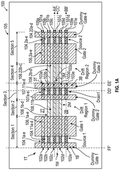
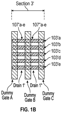
A finfet with lateral charge balance at the drain drift region
PatentWO2021257311A1
Innovation
- The introduction of an extended drain finFET design with a drain drift region, enhanced portions, and lateral charge balance regions, which include specific conductivity types and dopant concentrations to concentrate current flow and enable higher operating potentials.


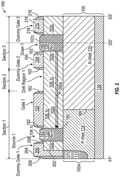
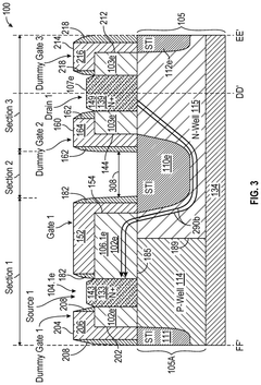
Fin-based field effect transistor (finFET) device with enhanced on-resistance and breakdown voltage
PatentActiveUS12113065B2
Innovation
- The implementation of a finFET device with a specific structure and fabrication flow that includes multiple alternating regions of n-type and p-type doped semiconductor, utilizing a super junction LDMOS structure, which allows for a lower Ron and higher breakdown voltage without additional mask or process steps, by optimizing the number and arrangement of fin portions in the drift regions.
Thermal Management Considerations
Thermal management represents a critical consideration in FinFET design, particularly when evaluating dimensions for power distribution. As FinFET technology continues to scale down, the power density increases significantly, leading to elevated thermal challenges that can compromise device performance and reliability. The three-dimensional structure of FinFETs, while beneficial for electrostatic control, creates unique thermal pathways that must be carefully managed.
The fin geometry directly impacts thermal dissipation capabilities. Taller and narrower fins, while advantageous for electrical performance, create thermal bottlenecks due to restricted cross-sectional areas for heat flow. This geometric constraint results in localized hotspots that can accelerate electromigration and time-dependent dielectric breakdown (TDDB) mechanisms, ultimately reducing device lifetime.
Material selection for thermal management plays a crucial role in FinFET design. The thermal conductivity of silicon decreases as dimensions approach the phonon mean free path (approximately 300nm at room temperature), creating additional challenges for heat dissipation in advanced nodes. Alternative fin materials such as SiGe or III-V compounds must be evaluated not only for their electrical properties but also for their thermal characteristics.
Heat dissipation pathways in FinFET structures follow complex three-dimensional routes. The primary thermal path typically runs from the channel through the fin to the substrate. Secondary paths include dissipation through metal contacts and interconnects. Optimizing these pathways requires careful consideration of dimensional parameters including fin height, width, and pitch, as well as gate length and oxide thickness.
Self-heating effects become increasingly pronounced as FinFET dimensions shrink. The temperature rise during operation can exceed 100°C above ambient in high-performance applications, significantly affecting carrier mobility and threshold voltage. Dynamic thermal management techniques, including adaptive body biasing and frequency scaling, must be incorporated into power distribution networks to mitigate these effects.
Thermal simulation methodologies for FinFETs require multi-physics approaches that couple electrical and thermal domains. Accurate modeling must account for temperature-dependent material properties, interface thermal resistances, and non-equilibrium heat transport phenomena at nanoscale dimensions. These simulations inform dimensional optimization strategies that balance electrical performance with thermal reliability.
The integration of FinFETs into three-dimensional packaging architectures introduces additional thermal management complexities. Through-silicon vias (TSVs) and microbumps create new thermal pathways that must be considered when evaluating fin dimensions for power distribution in advanced system-in-package solutions.
Semiconductor Fabrication Constraints
The fabrication of FinFET structures presents significant manufacturing challenges that directly impact power distribution capabilities. Current semiconductor fabrication processes operate at the 5nm to 3nm nodes, requiring extreme precision in fin dimensions. The height-to-width ratio of fins must be carefully controlled, with typical dimensions ranging from 30-50nm in height and 5-7nm in width. These precise measurements are critical as variations exceeding 0.5nm can dramatically alter transistor performance characteristics and power distribution profiles.
Lithography limitations represent a primary constraint in FinFET manufacturing. Even advanced extreme ultraviolet (EUV) lithography systems, operating at 13.5nm wavelengths, struggle with consistent fin formation below certain dimensions. This creates a fundamental physical barrier that impacts fin spacing and density, directly affecting power distribution network design and current-carrying capacity.
Material deposition uniformity presents another significant challenge. The conformal deposition of high-k dielectric materials and metal gates around the three-dimensional fin structures requires atomic-level precision. Variations in material thickness around the fin can create asymmetric electrical fields and uneven current distribution, leading to localized heating and reliability concerns in power delivery networks.
Etching processes for fin formation must achieve near-perfect anisotropy while maintaining atomic-level precision. The aspect ratio dependent etching (ARDE) effect becomes increasingly problematic as fin dimensions shrink, potentially creating non-uniform fin profiles that compromise electrical performance and power handling capabilities.
Doping uniformity around the three-dimensional fin structure presents unique challenges not encountered in planar technologies. Achieving consistent dopant profiles throughout the fin height is critical for uniform current flow and power distribution. Ion implantation shadowing effects and dopant diffusion variations can create regions of higher resistance that become bottlenecks in power delivery.
Thermal management constraints also significantly impact FinFET power distribution capabilities. The three-dimensional structure creates complex thermal pathways that must be carefully modeled and managed. Heat dissipation becomes increasingly challenging as fin density increases, potentially creating thermal hotspots that can compromise device reliability and power handling capacity.
These fabrication constraints collectively establish practical limits on minimum fin dimensions and maximum fin density, directly impacting the current-carrying capacity and power distribution capabilities of FinFET-based integrated circuits. As dimensions continue to shrink toward 2nm and beyond, these manufacturing challenges will increasingly define the practical limits of power distribution in advanced semiconductor devices.
Unlock deeper insights with PatSnap Eureka Quick Research — get a full tech report to explore trends and direct your research. Try now!
Generate Your Research Report Instantly with AI Agent
Supercharge your innovation with PatSnap Eureka AI Agent Platform!