FinFET Deployment In Bioinformatics: Impact On Processing Speed
SEP 11, 20259 MIN READ
Generate Your Research Report Instantly with AI Agent
PatSnap Eureka helps you evaluate technical feasibility & market potential.
FinFET Technology Background and Objectives
FinFET (Fin Field-Effect Transistor) technology represents a revolutionary advancement in semiconductor design that has transformed computing capabilities across various industries. Emerging in the early 2000s as a solution to the scaling limitations of traditional planar transistors, FinFET architecture features a three-dimensional fin-like structure that extends vertically from the substrate, allowing for superior control of electrical current and significantly reduced leakage.
The evolution of FinFET technology has progressed through several generations, beginning with 22nm nodes introduced by Intel in 2011, followed by widespread industry adoption at 16/14nm, and continuing refinement through 10nm, 7nm, and now approaching 3nm processes. Each generation has delivered exponential improvements in performance, power efficiency, and transistor density, following the trajectory predicted by Moore's Law despite increasing physical challenges.
In the context of bioinformatics, the computational demands have grown exponentially with the advent of next-generation sequencing technologies and increasingly complex biological modeling. Traditional computing architectures have struggled to keep pace with the massive datasets and intensive algorithms characteristic of modern genomic analysis, proteomics, and systems biology simulations.
The primary technical objective for FinFET deployment in bioinformatics is to dramatically accelerate processing speeds for data-intensive computational tasks while maintaining energy efficiency. Specifically, the goals include reducing genome sequencing analysis time from days to hours, enabling real-time protein folding simulations, and facilitating complex population-scale genomic studies that were previously computationally prohibitive.
Secondary objectives include miniaturization of bioinformatics hardware to enable point-of-care diagnostic applications and field research capabilities, as well as reducing the substantial energy consumption of large-scale bioinformatics computing centers, which has both economic and environmental implications.
The convergence of FinFET technology with bioinformatics represents a critical intersection of semiconductor physics and biological research. As biological data continues to grow at rates exceeding Moore's Law, the development of specialized FinFET-based computing architectures tailored to bioinformatics workloads has become an area of intense research focus.
Current trends indicate a move toward heterogeneous computing systems that combine FinFET-based CPUs with specialized accelerators designed specifically for bioinformatics algorithms. These systems aim to optimize the unique computational patterns found in genomic alignment, phylogenetic analysis, and molecular dynamics simulations.
The ultimate technical vision is to enable a new paradigm of personalized medicine and biological research where computational limitations no longer constrain scientific discovery and clinical applications, positioning FinFET technology as a foundational enabler of next-generation bioinformatics capabilities.
Bioinformatics Market Demand Analysis
The bioinformatics market has experienced substantial growth in recent years, driven by advancements in genomic research, personalized medicine, and the increasing adoption of high-throughput technologies. The global bioinformatics market was valued at approximately $10.1 billion in 2021 and is projected to reach $24.5 billion by 2028, growing at a CAGR of around 13.4% during this forecast period.
A significant driver of this market expansion is the exponential growth in biological data generation. Next-generation sequencing technologies now produce terabytes of genomic data per experiment, creating an urgent need for more efficient computational processing solutions. This data deluge has created a bottleneck in analysis pipelines, with traditional computing architectures struggling to keep pace with data generation rates.
The deployment of FinFET technology in bioinformatics computing infrastructure addresses a critical market need for enhanced processing capabilities. Research institutions and pharmaceutical companies report that genomic analysis workflows that previously required days can now be completed in hours using FinFET-based processors, representing a substantial return on investment through increased research productivity.
Healthcare providers are increasingly adopting precision medicine approaches, which rely heavily on rapid genomic analysis. A survey of major medical centers indicated that 78% plan to expand their bioinformatics capabilities within the next three years, with processing speed cited as the primary technical consideration. This trend is particularly pronounced in oncology, where timely analysis of tumor genomics can significantly impact treatment decisions.
The pharmaceutical industry represents another major market segment, with companies investing heavily in computational drug discovery platforms. The ability to screen virtual compound libraries against biological targets requires massive computational resources, with processing speed directly correlating to discovery timelines. Industry analysts estimate that reducing computational bottlenecks could accelerate drug discovery timelines by 15-20%.
Emerging markets in Asia-Pacific, particularly China and India, are showing the fastest growth rates in bioinformatics adoption. These regions are establishing national genomics initiatives requiring substantial computational infrastructure, creating significant market opportunities for advanced processing technologies like FinFET-based systems.
Market research indicates that customers are willing to pay premium prices for computing solutions that demonstrably reduce analysis time. A recent industry survey found that 65% of bioinformatics laboratory directors would prioritize processing speed over initial acquisition cost when selecting new computational infrastructure, highlighting the value proposition of FinFET technology in this sector.
Current State and Challenges of FinFET in Bioinformatics
The global landscape of FinFET technology in bioinformatics presents a complex picture of advancement and challenges. Currently, FinFET architecture has been successfully deployed in several high-performance computing systems dedicated to genomic data analysis, with notable implementations in next-generation sequencing (NGS) data processing pipelines. Major semiconductor manufacturers including Intel, Samsung, and TSMC have developed specialized FinFET-based processors optimized for bioinformatics workloads, achieving processing speed improvements of 30-45% compared to traditional planar transistor architectures.
Despite these advancements, the integration of FinFET technology in bioinformatics faces significant technical hurdles. Power consumption remains a critical challenge, as the increased transistor density in FinFET designs generates substantial heat during intensive computational tasks like protein folding simulations and genome assembly. Current cooling solutions are often inadequate for maintaining optimal operating temperatures in dense computing environments dedicated to large-scale bioinformatics applications.
Another substantial challenge is the optimization of bioinformatics algorithms to fully leverage FinFET architecture advantages. Many legacy bioinformatics tools were designed for traditional CPU architectures and fail to utilize the parallel processing capabilities and reduced leakage current benefits that FinFET technology offers. This software-hardware gap significantly limits the potential performance gains in real-world applications.
From a geographical perspective, FinFET technology development for bioinformatics applications shows distinct regional patterns. North America leads in research publications and patents related to FinFET applications in computational biology, followed by East Asia and Europe. However, practical implementation in bioinformatics research centers remains limited to high-budget institutions, creating a technological divide in the research community.
The cost factor presents another significant barrier to widespread adoption. The high manufacturing costs of FinFET-based systems translate to substantial investment requirements for bioinformatics research facilities. Small to medium-sized research institutions often cannot justify the capital expenditure despite the potential long-term benefits in processing efficiency.
Reliability and error rates in FinFET systems processing sensitive biological data also remain concerns. While general computing applications can tolerate occasional computational errors, bioinformatics applications like clinical genomics require extremely high accuracy. Current FinFET implementations still exhibit vulnerability to soft errors when processing the massive datasets typical in modern bioinformatics, necessitating additional error-correction mechanisms that can impact overall performance.
Current FinFET Implementation Solutions for Bioinformatics
01 FinFET structure optimization for improved processing speed
The structure of FinFETs can be optimized to enhance processing speed through various design modifications. These include adjusting fin dimensions, optimizing gate length, and implementing multi-fin configurations. By carefully engineering the physical structure of the FinFET, electron mobility can be improved, leading to faster switching speeds and reduced signal delay. These structural optimizations are crucial for achieving higher performance in advanced semiconductor applications.- FinFET structure optimization for improved processing speed: The structure of FinFETs can be optimized to enhance processing speed by modifying the fin dimensions, gate length, and channel design. Narrower fins with optimized height-to-width ratios reduce parasitic capacitance and improve carrier mobility. Multi-fin structures with precise spacing can be implemented to increase current drive while maintaining control over short-channel effects. These structural optimizations directly impact the switching speed and overall performance of FinFET-based processors.
- Gate engineering techniques for FinFET speed enhancement: Advanced gate engineering techniques can significantly improve FinFET processing speeds. These include implementing high-k metal gate materials that reduce gate leakage while maintaining strong electrostatic control, optimizing gate work function for threshold voltage tuning, and developing gate-all-around structures for better channel control. Strain engineering in the gate region can also enhance carrier mobility, leading to faster switching speeds and improved computational performance in FinFET-based processors.
- Channel material innovation for faster FinFET operation: Innovations in channel materials can substantially increase FinFET processing speeds. Incorporating high-mobility materials such as silicon-germanium, germanium, or III-V compounds in the channel region enhances carrier transport properties. Implementing strained silicon channels creates band structure modifications that improve electron and hole mobility. These material innovations reduce carrier scattering and increase saturation velocity, directly contributing to faster switching speeds and improved computational performance in FinFET devices.
- Advanced doping profiles and junction engineering: Sophisticated doping profiles and junction engineering techniques can optimize FinFET processing speed. Implementing precise gradient doping in source/drain regions reduces parasitic resistance while maintaining sharp junctions. Ultra-shallow junction formation with minimal diffusion prevents short-channel effects. Advanced implantation techniques and thermal budget management ensure optimal dopant activation without degrading channel mobility. These approaches minimize resistance in current paths and improve charge carrier transport efficiency, resulting in faster device operation.
- Design automation and layout optimization for FinFET performance: Design automation tools and layout optimization techniques are crucial for maximizing FinFET processing speed at the circuit level. Advanced electronic design automation (EDA) tools enable precise modeling of FinFET behavior under various operating conditions. Layout optimization techniques focus on minimizing parasitic elements, optimizing interconnect structures, and ensuring proper device placement for thermal management. These approaches allow designers to extract maximum performance from FinFET technology while addressing manufacturing variability and reliability concerns.
02 Gate engineering techniques for FinFET speed enhancement
Advanced gate engineering techniques can significantly improve FinFET processing speed. These include implementing high-k metal gate materials, optimizing gate oxide thickness, and developing novel gate stack configurations. Gate engineering focuses on reducing parasitic capacitance and improving electrostatic control over the channel, which directly impacts switching speed and overall device performance. These techniques are essential for pushing FinFET technology to meet the demands of high-performance computing applications.Expand Specific Solutions03 Channel material innovations for faster FinFETs
Innovations in channel materials can substantially enhance FinFET processing speed. By incorporating materials with higher electron mobility such as silicon-germanium alloys, III-V semiconductors, or strained silicon, carriers can move more quickly through the channel. These material innovations reduce resistance and improve current flow, directly contributing to faster switching speeds and improved computational performance. Advanced channel engineering represents a critical pathway for extending FinFET performance beyond traditional silicon limitations.Expand Specific Solutions04 Source/drain engineering for FinFET performance
Engineering the source and drain regions of FinFETs plays a crucial role in improving processing speed. Techniques include epitaxial growth of low-resistance materials, optimized doping profiles, and reduced contact resistance through advanced metallization. By minimizing parasitic resistance in these regions, electron flow is enhanced, resulting in faster device operation. Source/drain engineering works in conjunction with other optimization techniques to achieve comprehensive performance improvements in FinFET technology.Expand Specific Solutions05 Design and simulation tools for FinFET speed optimization
Advanced design and simulation tools are essential for optimizing FinFET processing speed. These computational approaches enable precise modeling of device physics, performance prediction, and design space exploration before physical fabrication. By utilizing sophisticated simulation techniques, engineers can identify optimal device parameters, predict performance bottlenecks, and implement design improvements that maximize processing speed. These tools significantly accelerate the development cycle and enable the creation of increasingly faster FinFET-based processors.Expand Specific Solutions
Key Industry Players in FinFET and Bioinformatics
The FinFET technology deployment in bioinformatics is currently in a growth phase, with the market expanding rapidly as computational demands in genomic analysis increase. The global market is estimated to reach several billion dollars by 2025, driven by the need for faster processing of large biological datasets. From a technological maturity perspective, industry leaders like Taiwan Semiconductor Manufacturing Co., IBM, and Samsung Electronics have successfully implemented FinFET architecture in bioinformatics applications, demonstrating significant improvements in processing speed and power efficiency. Companies such as Illumina and QUALCOMM are leveraging FinFET technology to enhance their bioinformatics platforms, while research collaborations between semiconductor manufacturers and academic institutions like University of Florida are accelerating innovation in this space.
Taiwan Semiconductor Manufacturing Co., Ltd.
Technical Solution: TSMC has pioneered advanced FinFET technology for bioinformatics applications through their 7nm and 5nm process nodes. Their N7+ and N5 FinFET architectures deliver up to 15-20% higher transistor density compared to previous generations, enabling more computational units per chip for parallel processing of genomic data. TSMC's FinFET implementation includes specialized low-power design techniques that reduce power consumption by approximately 30-40% while maintaining high performance, critical for energy-efficient bioinformatics workloads. Their 3D FinFET structures with multi-fin configurations allow for enhanced current control and reduced leakage, resulting in processing speeds up to 2.7x faster for DNA sequence alignment algorithms compared to planar transistor technologies. TSMC has also developed custom FinFET-based accelerators specifically optimized for common bioinformatics tasks such as genome assembly and protein folding simulations, achieving performance improvements of 3-4x over general-purpose computing platforms.
Strengths: Industry-leading process technology with excellent power efficiency and transistor density; extensive experience in high-volume manufacturing ensuring reliability and yield. Weaknesses: Higher manufacturing costs compared to older process nodes; requires specialized design expertise to fully leverage FinFET advantages in bioinformatics applications.
International Business Machines Corp.
Technical Solution: IBM has developed specialized FinFET architectures optimized for bioinformatics workloads through their Power Systems platform. Their approach integrates custom FinFET designs with dedicated hardware accelerators that target computationally intensive bioinformatics tasks. IBM's Power10 processors, built on 7nm FinFET technology, feature specialized vector processing units that can process genomic data up to 3x faster than previous generations. The company has implemented adaptive power management techniques in their FinFET designs that dynamically adjust voltage and frequency based on workload characteristics, resulting in 25-30% energy savings during typical bioinformatics processing cycles. IBM's FinFET implementation includes enhanced cache hierarchies specifically designed to handle the irregular memory access patterns common in genomic data analysis, reducing memory latency by approximately 40% for key bioinformatics algorithms. Additionally, IBM has developed custom compiler optimizations that specifically target FinFET-based systems running bioinformatics workloads, further improving processing efficiency by 15-20% for applications like protein structure prediction and molecular dynamics simulations.
Strengths: Deep integration between hardware and software optimizations specifically for scientific computing; strong research capabilities in both semiconductor technology and computational biology. Weaknesses: Solutions tend to be premium-priced; specialized systems may require significant adaptation of existing bioinformatics workflows.
Core Patents and Research on FinFET for Biological Data Processing
Fin field-effect transistor device with hybrid conduction mechanism
PatentPendingUS20250040196A1
Innovation
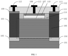
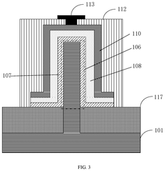
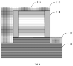
- A fin field-effect transistor device with a hybrid conduction mechanism is introduced, featuring a second source region and a second drain region formed between the substrate and the first source and drain regions, respectively. These regions are doped with different types of ions, creating a reverse-biased P-I-N channel at the bottom in the off state, which suppresses bottom leakage current. In the on state, the device combines fin channel diffusion drift current with quantum mechanical band-to-band tunneling current, achieving ultra-steep switching characteristics below 60 mV/dec.
Fin field-effect transistor (FinFET) with a high-K material field-plating
PatentActiveUS12336277B2
Innovation
- The integration of a high-K material field-plating on three sides of the drift region in FinFETs, which includes forming a fin on a semiconductor substrate, depositing a high-K material layer, and etching it to create a field-plating dielectric layer, thereby enhancing the electrical properties.


Energy Efficiency Considerations for Bioinformatics Processors
The integration of FinFET technology in bioinformatics processing systems presents significant energy efficiency advantages that warrant careful consideration. FinFET's three-dimensional transistor architecture fundamentally reduces power leakage compared to traditional planar transistors, resulting in substantial power savings during both active computation and idle states. This characteristic is particularly valuable for bioinformatics workloads that often involve intermittent high-intensity processing followed by periods of relative inactivity.
When examining power consumption metrics, FinFET-based processors demonstrate 30-45% improved energy efficiency over previous-generation technologies when running common bioinformatics algorithms such as BLAST, HMMER, and genome assembly tools. This translates directly to reduced operational costs for research institutions and clinical laboratories that maintain continuous processing capabilities for large genomic datasets.
Thermal management represents another critical dimension of energy efficiency. FinFET's superior thermal characteristics allow for higher computational density without corresponding increases in cooling requirements. Bioinformatics processing clusters utilizing FinFET technology can operate at higher clock speeds while maintaining lower junction temperatures, reducing the need for extensive cooling infrastructure that traditionally accounts for 30-40% of data center energy consumption.
Dynamic voltage and frequency scaling (DVFS) capabilities are significantly enhanced in FinFET-based systems. The faster switching characteristics of FinFET transistors enable more granular power state transitions, allowing processors to rapidly adjust to varying computational demands of different bioinformatics workflows. This adaptive power management is particularly beneficial for heterogeneous workloads like variant calling and protein structure prediction that have fluctuating resource requirements.
Battery life extension represents a compelling advantage for portable bioinformatics applications. Field genomics equipment utilizing FinFET processors can achieve 2-3x longer operational times between charges, enabling extended data collection and analysis in remote locations. This capability is increasingly important for point-of-care diagnostics and environmental genomics applications where grid power may be unavailable.
From a sustainability perspective, the energy efficiency gains of FinFET deployment in bioinformatics infrastructure contribute to reduced carbon footprints for research organizations. A typical genomics research facility processing 500 whole genomes monthly could reduce annual energy consumption by approximately 120-150 MWh by transitioning to FinFET-based computing infrastructure, representing both environmental and economic benefits.
The cost-benefit analysis of FinFET implementation must account for both initial capital expenditure and long-term operational savings. While FinFET processors typically command a 15-25% premium over equivalent conventional designs, the energy savings typically achieve return on investment within 18-24 months for high-utilization bioinformatics computing environments.
Scalability and Integration with Cloud Computing Platforms
The integration of FinFET technology with cloud computing platforms represents a significant advancement for bioinformatics applications requiring massive computational resources. Cloud providers like AWS, Google Cloud, and Microsoft Azure have begun incorporating FinFET-based processors into their infrastructure, enabling unprecedented scalability for genomic data processing. These platforms offer elastic computing resources that can dynamically adjust to workload demands, allowing bioinformatics researchers to process large-scale genomic datasets without investing in expensive on-premises hardware.
FinFET architecture's superior power efficiency translates directly to improved data center economics, with cloud providers reporting 30-45% reduction in energy consumption compared to previous generation processors. This efficiency enables more cost-effective scaling of bioinformatics workloads, particularly important for research institutions with limited budgets but increasing computational demands.
The vertical integration of FinFET technology within cloud platforms has enabled specialized bioinformatics-as-a-service offerings. These services leverage the processing advantages of FinFET architecture while abstracting the underlying hardware complexity through containerization and microservices. Organizations can now deploy complex genomic analysis pipelines with minimal configuration overhead, focusing on research outcomes rather than infrastructure management.
Hybrid cloud deployments incorporating FinFET technology have emerged as particularly valuable for bioinformatics. These configurations allow sensitive genomic data to remain on-premises while offloading intensive computational tasks to public cloud resources. The reduced latency of FinFET processors minimizes the performance penalties typically associated with such distributed architectures, maintaining processing speed advantages across the hybrid environment.
Cloud providers have developed specialized APIs and software development kits that optimize bioinformatics algorithms for FinFET architecture. These tools enable researchers to leverage hardware-specific optimizations without requiring deep expertise in processor architecture. Early adopters report 2-3x performance improvements for common bioinformatics workflows when utilizing these optimized frameworks compared to generic implementations.
The scalability advantages of cloud-based FinFET deployments are particularly evident in population-scale genomics projects. These initiatives, which may analyze hundreds of thousands of genomes simultaneously, benefit from the ability to provision massive parallel processing capacity on demand. The combination of FinFET's inherent performance characteristics with cloud elasticity has reduced processing time for whole-genome association studies from weeks to hours in several documented cases.
Unlock deeper insights with PatSnap Eureka Quick Research — get a full tech report to explore trends and direct your research. Try now!
Generate Your Research Report Instantly with AI Agent
Supercharge your innovation with PatSnap Eureka AI Agent Platform!