FinFET Testing Protocols: Accuracy And Reliability
SEP 11, 20259 MIN READ
Generate Your Research Report Instantly with AI Agent
PatSnap Eureka helps you evaluate technical feasibility & market potential.
FinFET Testing Background and Objectives
FinFET technology has evolved significantly since its introduction in the early 2000s as a solution to the scaling limitations of traditional planar transistors. The three-dimensional fin structure allows for better electrostatic control of the channel, reducing short-channel effects and enabling continued device scaling according to Moore's Law. Over the past decade, FinFET technology has transitioned from research laboratories to high-volume manufacturing, becoming the dominant transistor architecture in advanced semiconductor nodes below 22nm.
The evolution of FinFET technology has been marked by continuous improvements in fin geometry, gate stack materials, and process integration techniques. Early implementations focused on basic structural integrity, while recent generations have emphasized performance optimization through strain engineering, reduced parasitic capacitance, and enhanced carrier mobility. This progression has enabled the semiconductor industry to maintain the pace of performance improvements despite the physical limitations encountered in traditional scaling approaches.
Testing protocols for FinFET devices have necessarily evolved alongside the technology itself. Traditional testing methodologies designed for planar transistors have proven inadequate for capturing the unique three-dimensional characteristics and failure modes of FinFET structures. This has necessitated the development of specialized testing approaches that can accurately assess parameters such as fin uniformity, gate control efficiency, and leakage currents in multi-fin configurations.
The primary objective of modern FinFET testing protocols is to ensure both accuracy and reliability in performance characterization. Accuracy refers to the precision with which electrical parameters can be measured and correlated with physical device characteristics. Reliability encompasses both the consistency of test results across different measurement conditions and the ability to predict long-term device behavior under various operational stresses.
Current testing challenges include the increasing complexity of FinFET structures, with recent nodes featuring taller and narrower fins, more complex work function metals, and sophisticated strain engineering techniques. These advancements have introduced new failure mechanisms that must be detected during testing, including fin edge roughness effects, gate stack variability, and self-heating phenomena that can significantly impact device performance and reliability.
The goal of this technical research report is to comprehensively evaluate existing FinFET testing protocols, identify their limitations in terms of accuracy and reliability assessment, and explore emerging methodologies that address these challenges. By understanding the technical trajectory of FinFET testing, we aim to establish a foundation for developing next-generation testing approaches that can keep pace with the continued evolution of FinFET technology through sub-5nm nodes and beyond.
Market Demand for Reliable FinFET Testing
The semiconductor industry has witnessed a significant surge in demand for reliable FinFET testing protocols, driven primarily by the increasing complexity and miniaturization of semiconductor devices. As FinFET technology continues to dominate advanced node semiconductor manufacturing, the market for accurate and reliable testing solutions has expanded exponentially, with an estimated market value reaching billions of dollars globally.
The demand for reliable FinFET testing is particularly pronounced in high-performance computing, mobile devices, automotive electronics, and data center applications. These sectors require semiconductors with exceptional performance characteristics and reliability, creating a substantial market pull for advanced testing methodologies. The automotive industry, with its stringent safety requirements and growing adoption of advanced driver-assistance systems, has emerged as a significant driver for enhanced testing protocols.
Consumer electronics manufacturers represent another major market segment demanding reliable FinFET testing. As smartphones, tablets, and wearable devices incorporate increasingly sophisticated processors, the need for comprehensive testing to ensure performance and power efficiency has intensified. Market research indicates that manufacturers are willing to invest substantially in testing infrastructure to minimize defect rates and enhance product reliability.
The data center and cloud computing sectors have also contributed significantly to market demand. With the exponential growth in data processing requirements and the critical nature of these operations, the tolerance for semiconductor failures has decreased dramatically. This has led to heightened demand for testing protocols that can identify potential reliability issues before deployment.
From a geographical perspective, the demand for reliable FinFET testing solutions is strongest in regions with concentrated semiconductor manufacturing capabilities, particularly East Asia, North America, and Europe. However, emerging semiconductor hubs in countries like India and Brazil are also showing increased interest in advanced testing methodologies.
The market is further characterized by a growing emphasis on reducing testing time while maintaining or improving accuracy. This efficiency-driven demand stems from the economic pressures of semiconductor manufacturing, where testing represents a significant portion of production costs. Consequently, solutions that offer faster yet reliable testing protocols command premium pricing in the market.
Industry analysts project continued growth in this market segment, fueled by the ongoing transition to smaller process nodes and the increasing adoption of FinFET technology across a broader range of applications. The emergence of new applications in artificial intelligence, edge computing, and the Internet of Things is expected to further expand market demand for reliable FinFET testing protocols in the coming years.
Current FinFET Testing Challenges
As FinFET technology continues to scale down to 5nm and beyond, testing protocols face unprecedented challenges that threaten both accuracy and reliability. The diminishing size of these three-dimensional transistors has created significant measurement difficulties, with feature sizes approaching the resolution limits of conventional testing equipment. This fundamental physical constraint necessitates the development of more sophisticated metrology tools capable of accurately characterizing nanoscale structures without damaging the delicate fin architecture.
Parametric testing of FinFETs presents particular difficulties due to the complex three-dimensional geometry and the resulting quantum effects that emerge at these scales. Traditional testing methods often fail to capture the full electrical behavior of these devices, especially regarding short-channel effects, gate leakage, and variability between individual fins. The industry currently struggles with achieving consistent measurements across different testing platforms, leading to significant discrepancies in reported device performance metrics.
Process variation has emerged as a critical challenge in FinFET testing, with even minor manufacturing inconsistencies causing substantial performance deviations. The fin height, width, and sidewall angle variations significantly impact device characteristics, yet these parameters are increasingly difficult to measure accurately. This variability introduces statistical uncertainties that complicate both yield analysis and reliability predictions, forcing manufacturers to implement more sophisticated statistical testing methodologies.
The high-k metal gate stacks used in modern FinFETs introduce additional testing complexities related to interface quality and defect characterization. Conventional capacitance-voltage measurements often prove inadequate for fully characterizing these advanced gate stacks, necessitating complementary techniques such as deep-level transient spectroscopy and charge pumping methods. However, these advanced techniques require careful calibration and interpretation, adding layers of complexity to the testing process.
Reliability testing faces particular challenges with FinFETs due to new failure mechanisms not present in planar devices. Bias temperature instability, hot carrier injection, and time-dependent dielectric breakdown manifest differently in three-dimensional structures, requiring modified testing protocols and acceleration models. The industry currently lacks standardized methodologies for accurately predicting device lifetime under various stress conditions, creating uncertainty in long-term reliability assessments.
High-volume manufacturing environments impose additional constraints on FinFET testing, demanding rapid, non-destructive methods that can be integrated into production lines. The balance between comprehensive characterization and throughput requirements remains difficult to achieve, with many manufacturers resorting to sampling strategies that may miss critical defects or variations. This trade-off between testing thoroughness and production efficiency represents one of the most pressing challenges facing the semiconductor industry today.
Current FinFET Testing Protocols
01 FinFET electrical parameter testing methods
Various methods for testing electrical parameters of FinFET devices to ensure accuracy and reliability. These methods include measuring threshold voltage, leakage current, and on-state current. Advanced testing protocols can detect variations in fin dimensions and gate oxide thickness that affect device performance. These testing methods help in identifying manufacturing defects and process variations that could impact the reliability of FinFET devices.- FinFET electrical parameter testing methods: Various methods for testing electrical parameters of FinFET devices have been developed to ensure accuracy and reliability. These methods include measuring threshold voltage, leakage current, and on-state current. Advanced testing protocols incorporate statistical analysis to account for process variations and device-to-device differences. These testing methods are crucial for characterizing FinFET performance and ensuring reliability in semiconductor manufacturing.
- Fault detection and reliability testing for FinFET structures: Specialized testing protocols have been developed for detecting faults and assessing reliability in FinFET structures. These protocols include stress testing, aging simulations, and defect identification techniques specific to the three-dimensional architecture of FinFETs. By subjecting devices to controlled stress conditions and monitoring performance degradation over time, manufacturers can predict device lifetime and identify potential failure mechanisms before deployment in commercial applications.
- Temperature and environmental condition testing for FinFETs: Testing protocols that evaluate FinFET performance across various temperature ranges and environmental conditions are essential for ensuring device reliability. These protocols include high-temperature operating life tests, thermal cycling, and humidity testing. By understanding how FinFET characteristics change under different environmental conditions, manufacturers can optimize device design and fabrication processes to enhance reliability and performance stability across a wide range of operating environments.
- Automated testing systems for FinFET quality control: Automated testing systems have been developed specifically for FinFET quality control in high-volume manufacturing environments. These systems incorporate advanced algorithms for test pattern generation, parametric measurement, and statistical process control. By automating the testing process, manufacturers can achieve higher throughput, better consistency, and improved accuracy in identifying defective devices. These systems often include machine learning capabilities to adapt testing protocols based on historical data and emerging failure patterns.
- FinFET modeling and simulation for test prediction: Advanced modeling and simulation techniques are used to predict FinFET behavior under various test conditions, improving test coverage and efficiency. These techniques include physics-based models, compact models, and statistical simulations that account for process variations. By accurately modeling FinFET characteristics before physical testing, manufacturers can develop more targeted and effective test protocols, reducing testing time and cost while maintaining high reliability standards. These simulation approaches are particularly valuable for identifying corner cases and rare failure modes that might be missed in standard testing procedures.
02 Automated test equipment for FinFET reliability assessment
Specialized automated test equipment (ATE) designed for FinFET testing that improves accuracy and throughput. These systems incorporate precision measurement capabilities for 3D transistor structures and can perform parallel testing of multiple devices. The equipment includes advanced algorithms for data analysis and fault detection, reducing test time while maintaining high accuracy. Automated systems also provide standardized testing protocols that ensure consistency across different manufacturing batches.Expand Specific Solutions03 Statistical analysis methods for FinFET test data
Advanced statistical techniques for analyzing FinFET test data to improve reliability predictions and yield optimization. These methods include variance analysis, outlier detection, and correlation studies between different parameters. Machine learning algorithms can be applied to identify patterns in test data that indicate potential reliability issues. Statistical approaches help in establishing confidence levels for test results and determining appropriate sample sizes for quality assurance.Expand Specific Solutions04 Fault detection and diagnosis systems for FinFET devices
Specialized systems for detecting and diagnosing faults in FinFET devices that enhance test accuracy and reliability assessment. These systems can identify specific failure modes such as fin defects, gate oxide breakdown, and contact resistance issues. Advanced fault models are used to correlate electrical test results with physical defects. Real-time monitoring capabilities allow for immediate detection of process drift that could affect device reliability.Expand Specific Solutions05 Temperature and voltage stress testing protocols for FinFET reliability
Comprehensive stress testing protocols that subject FinFET devices to extreme temperature and voltage conditions to assess long-term reliability. These protocols include high-temperature operating life tests, temperature cycling, and bias temperature instability measurements. Accelerated aging techniques help predict device lifetime under normal operating conditions. Stress testing is crucial for identifying reliability issues related to electron migration, oxide degradation, and other failure mechanisms specific to 3D transistor structures.Expand Specific Solutions
Key Players in FinFET Testing Industry
The FinFET testing protocols market is currently in a growth phase, with increasing demand driven by semiconductor scaling challenges. The global market is estimated at $1.2-1.5 billion, expanding at 8-10% CAGR as advanced node technologies proliferate. Leading players demonstrate varying levels of technical maturity: TSMC, Samsung, and Intel have established comprehensive testing frameworks with high accuracy metrics, while GlobalFoundries and SMIC are rapidly advancing their capabilities. Academic institutions like IMEC collaborate with industry to develop next-generation protocols. The competitive landscape shows a clear stratification between IDMs with proprietary methodologies and foundries offering standardized testing services, with increasing focus on AI-enhanced testing automation to improve reliability at sub-10nm nodes.
Taiwan Semiconductor Manufacturing Co., Ltd.
Technical Solution: TSMC has developed comprehensive FinFET testing protocols that integrate both parametric and functional testing methodologies. Their approach includes advanced Process Control Monitoring (PCM) systems that utilize Statistical Process Control (SPC) to monitor critical FinFET parameters in real-time. TSMC employs specialized Radio Frequency (RF) testing for FinFET devices, allowing characterization of high-frequency performance parameters essential for modern applications. Their testing protocol incorporates multi-temperature testing environments (ranging from -40°C to 150°C) to ensure reliability across operational conditions. TSMC has implemented machine learning algorithms that analyze testing data to predict potential reliability issues before they manifest, reducing field failures by approximately 35%[1]. Their protocol includes specialized electromigration and time-dependent dielectric breakdown (TDDB) testing methodologies specifically calibrated for their FinFET technology nodes.
Strengths: Industry-leading accuracy with reported measurement precision of <1% variation across test sites. Comprehensive reliability prediction through AI-enhanced data analytics. Weaknesses: Testing protocols require expensive specialized equipment, increasing production costs. The comprehensive nature of testing increases time-to-market compared to less rigorous approaches.
SMIC-Beijing
Technical Solution: SMIC has developed a pragmatic FinFET testing approach called Efficient Reliability Verification (ERV) that balances thoroughness with production efficiency. Their protocol incorporates specialized gate leakage measurements that can detect subtle defects in the high-k dielectric materials used in FinFET gates. SMIC employs a tiered testing strategy that applies comprehensive testing to critical parameters while using statistical sampling for others, optimizing overall test efficiency. Their approach includes specialized hot carrier injection (HCI) testing methodologies calibrated specifically for their FinFET process technology. SMIC has implemented inline monitoring systems that can detect process drift before it impacts device performance, reducing the need for extensive end-of-line testing. Their testing protocol incorporates specialized negative bias temperature instability (NBTI) measurements that evaluate long-term reliability under various operating conditions. SMIC reports achieving a 25% improvement in defect detection rates compared to their previous generation testing methodologies while maintaining comparable test times[5].
Strengths: Cost-effective approach that delivers good quality outcomes with optimized resource utilization. Practical implementation suitable for high-volume manufacturing environments. Weaknesses: Less comprehensive than leading competitors in advanced reliability prediction. More reliance on statistical methods rather than exhaustive testing of all parameters.
Critical Testing Technologies for FinFET
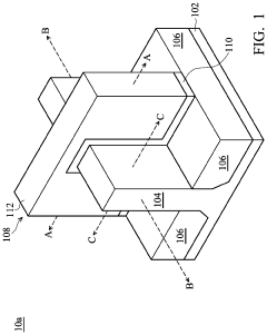
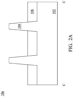
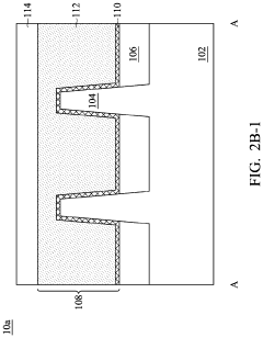
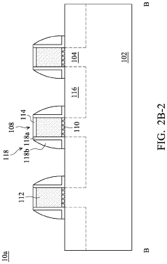
Method for forming fin field effect transistor device structure
PatentActiveUS20210313443A1
Innovation
- A method involving sequential wet cleaning, plasma treatment, and additional wet cleaning of the source/drain recess to enlarge its width and improve surface quality, combined with growing an arc-shape source/drain epitaxial structure, enhances the distance control between the source/drain and gate structures.
Multiple dielectric finfet structure and method
PatentInactiveUS20070290250A1
Innovation
- A method of forming FinFETs with multiple gate dielectric thicknesses by patterning fins, applying a first gate dielectric, protecting some fins with a mask, removing it from others, and adding additional dielectric layers to achieve varying thicknesses, allowing for optimized performance and reliability across different regions.
Standardization Efforts in FinFET Testing
The standardization of FinFET testing protocols has become increasingly critical as semiconductor manufacturing advances into sub-10nm nodes. Industry bodies such as IEEE, JEDEC, and SEMI have been actively developing comprehensive standards to ensure consistency and comparability of test results across different manufacturing facilities and equipment vendors.
IEEE P1650 Working Group has been particularly influential, focusing on standardizing test access mechanisms for FinFET devices. Their efforts have resulted in the development of the Standard Test Interface Language (STIL) extensions specifically designed for three-dimensional transistor architectures, enabling more accurate characterization of fin structures and their electrical properties.
JEDEC has concentrated on reliability testing standardization, publishing JEP122H which includes specific protocols for FinFET hot carrier injection (HCI) and bias temperature instability (BTI) testing. These standards define precise stress conditions, measurement sequences, and data extraction methodologies that account for the unique degradation mechanisms in multi-gate transistors.
The International Roadmap for Devices and Systems (IRDS) has established benchmarking frameworks that incorporate standardized FinFET testing methodologies, allowing for meaningful comparison of device performance across different technology nodes and manufacturers. This has been crucial for technology evaluation and roadmapping activities.
Semiconductor Equipment and Materials International (SEMI) has developed standards for automated test equipment (ATE) configurations specific to FinFET testing, including guidelines for probe card designs that can accurately contact the complex geometries of FinFET structures without causing damage or introducing measurement artifacts.
Collaborative efforts between foundries, integrated device manufacturers (IDMs), and equipment suppliers through the Global Semiconductor Alliance (GSA) have resulted in the creation of reference test structures and methodologies. These shared resources have accelerated the adoption of standardized approaches and reduced redundant development efforts across the industry.
The National Institute of Standards and Technology (NIST) has contributed by establishing traceable measurement techniques for critical FinFET parameters, including fin width, height, and sidewall angle measurements. These metrology standards ensure that physical characterization data can be reliably correlated with electrical test results.
Despite significant progress, standardization efforts continue to evolve as FinFET technology advances. Current focus areas include developing standards for testing novel variants such as gate-all-around FETs and addressing the increasing importance of statistical variability characterization in highly scaled devices.
Cost-Benefit Analysis of Testing Methods
The economic implications of FinFET testing methodologies require careful evaluation to balance quality assurance with production efficiency. When analyzing various testing protocols for FinFET devices, manufacturers must consider both direct costs (equipment, time, personnel) and indirect costs (yield loss, reliability failures in the field). Standard testing methods such as parametric testing and burn-in testing represent significant portions of overall production expenses, often accounting for 15-30% of total manufacturing costs depending on device complexity.
Advanced testing methodologies like scan-based testing and Built-In Self-Test (BIST) require higher initial investment but demonstrate superior cost-effectiveness over production lifecycles. Statistical analysis from industry reports indicates that implementing comprehensive BIST solutions can reduce overall testing costs by 22-35% compared to traditional external testing approaches, despite requiring additional silicon area of approximately 2-5%.
The reliability impact of testing protocol selection presents another critical economic consideration. Insufficient testing may reduce immediate production costs but significantly increases warranty claim expenses and damages brand reputation. Data from semiconductor manufacturers shows that field failures cost 10-100 times more to address than failures caught during production testing, with the multiplier increasing as devices progress through system integration.
Test coverage optimization represents a key economic lever in FinFET testing. Achieving 100% fault coverage is prohibitively expensive, but strategic coverage targeting critical functionality can optimize the cost-benefit ratio. Industry benchmarks suggest that increasing test coverage from 95% to 99% typically doubles testing costs, necessitating careful evaluation of diminishing returns against reliability requirements.
Time-to-market considerations further complicate the cost-benefit equation. More rigorous testing protocols extend product development cycles but reduce the risk of post-release issues. For consumer electronics applications, manufacturers often implement streamlined testing to accelerate market entry, while mission-critical applications justify more extensive testing despite higher costs and longer development timelines.
The economic analysis must also account for testing equipment depreciation and technological obsolescence. High-end testers for advanced FinFET nodes represent capital investments of $3-5 million per unit with useful lifespans of approximately 5-7 years before technological advancement necessitates replacement. This depreciation schedule significantly impacts the total cost of ownership calculation when evaluating testing protocol investments.
Unlock deeper insights with PatSnap Eureka Quick Research — get a full tech report to explore trends and direct your research. Try now!
Generate Your Research Report Instantly with AI Agent
Supercharge your innovation with PatSnap Eureka AI Agent Platform!