FinFET Utilization In IoT: Energy Optimization
SEP 11, 202510 MIN READ
Generate Your Research Report Instantly with AI Agent
PatSnap Eureka helps you evaluate technical feasibility & market potential.
FinFET Technology Evolution and Energy Efficiency Goals
FinFET technology has undergone significant evolution since its introduction in the early 2000s. Initially developed to address the scaling limitations of planar transistors, FinFETs represented a revolutionary shift in semiconductor architecture by implementing a three-dimensional structure. The first commercial FinFET processes were introduced at the 22nm node by Intel in 2011, marking a pivotal moment in transistor design. This transition was driven by the need to mitigate short-channel effects and reduce leakage current, which had become increasingly problematic as transistor dimensions shrank below 28nm.
The evolution trajectory of FinFET technology has been characterized by continuous refinement in fin geometry, gate stack engineering, and channel material innovation. From 2011 to 2015, the industry witnessed the transition from 22nm to 14nm FinFETs, with improvements in fin pitch, height-to-width ratio, and gate length control. Between 2016 and 2020, further scaling to 10nm and 7nm nodes brought enhanced performance and power efficiency through strain engineering and advanced lithography techniques.
In the context of IoT applications, FinFET technology evolution has increasingly focused on energy optimization rather than pure performance gains. This shift reflects the unique requirements of IoT devices, which prioritize extended battery life and energy autonomy over computational throughput. The technical goals for FinFET utilization in IoT center around achieving ultra-low standby power, efficient operation at near-threshold voltages, and optimized performance-per-watt metrics.
Current energy efficiency goals for FinFET implementation in IoT applications include reducing static power consumption to sub-nanowatt levels per transistor, enabling operation at supply voltages below 0.5V without significant performance degradation, and achieving dynamic power scaling that responds intelligently to workload variations. These goals necessitate innovations in circuit design techniques, including power gating, body biasing, and adaptive voltage scaling specifically tailored for FinFET characteristics.
Looking forward, the technology roadmap for FinFETs in IoT applications aims to achieve a 10x improvement in energy efficiency by 2025 compared to 2020 baselines. This ambitious target requires holistic optimization across device, circuit, and system levels. Emerging research directions include hybrid FinFET designs that incorporate tunnel FET principles for steeper subthreshold slopes, integration with energy harvesting technologies, and co-optimization with specialized IoT workloads.
The ultimate technical objective is to enable a new generation of IoT devices that can operate for years on a single battery charge or even achieve energy autonomy through ambient energy harvesting. This vision requires pushing FinFET technology beyond conventional scaling approaches toward designs specifically optimized for the ultra-low power envelope of distributed IoT sensing and computing applications.
IoT Market Demand for Low-Power Semiconductors
The Internet of Things (IoT) market has witnessed exponential growth in recent years, with the number of connected devices projected to reach 30.9 billion by 2025. This proliferation of IoT devices has created a substantial and rapidly expanding demand for low-power semiconductor solutions. Energy efficiency has become a critical factor in IoT applications, as most devices operate on limited power sources such as batteries or energy harvesting systems.
The market for low-power semiconductors in IoT applications is primarily driven by the need for extended battery life in remote and mobile devices. End-users across industrial, consumer, healthcare, and smart city applications increasingly demand devices that can operate for months or years without battery replacement. This requirement has transformed energy efficiency from a mere feature to a fundamental market differentiator.
Consumer IoT devices, including wearables and smart home products, represent the largest segment demanding low-power semiconductors. These devices typically operate on small batteries and must maintain connectivity for extended periods while performing increasingly complex functions. The wearable technology market alone is growing at 15.9% annually, with power consumption being the primary technical constraint cited by manufacturers.
Industrial IoT applications present another significant market segment, where sensors and monitoring devices are often deployed in remote or hazardous locations. In these scenarios, the cost and logistical challenges of battery replacement make ultra-low-power operation essential. The industrial IoT market is expected to grow at 16.7% annually through 2026, with energy-efficient semiconductors being a key enabling technology.
Edge computing represents an emerging trend in IoT architecture that further drives demand for energy-efficient processing capabilities. As more computational tasks shift from centralized cloud servers to edge devices, the need for semiconductors that can perform complex operations with minimal power consumption becomes increasingly critical. Market analysis indicates that 75% of enterprise-generated data will be processed at the edge by 2025, up from 10% in 2018.
The healthcare IoT segment demonstrates particularly stringent requirements for low-power operation, especially in implantable and wearable medical devices. These applications demand not only minimal power consumption but also reliable performance and long-term stability, creating premium market opportunities for advanced semiconductor technologies like FinFET.
Regional analysis shows that Asia-Pacific currently leads in IoT semiconductor consumption, followed by North America and Europe. However, the fastest growth is occurring in emerging markets where infrastructure limitations make energy efficiency particularly valuable. This global expansion is creating diverse market requirements that semiconductor manufacturers must address with scalable, power-optimized solutions.
Current FinFET Implementation Challenges in IoT Devices
Despite the promising advantages of FinFET technology for IoT applications, several significant implementation challenges currently impede its widespread adoption in energy-constrained IoT devices. The primary obstacle remains the complex manufacturing process, which requires sophisticated lithography techniques and precise control over three-dimensional structures. This complexity translates directly into higher production costs, making FinFET integration prohibitively expensive for low-cost IoT devices that operate on tight profit margins.
The scaling limitations present another critical challenge. While FinFETs offer excellent performance at 14nm and below, many IoT applications do not require such advanced nodes and cannot justify the associated costs. The industry faces difficulties in developing optimized FinFET designs specifically tailored for the 22-28nm nodes that would be more appropriate for IoT applications, creating a technological gap in the market.
Power management issues persist despite FinFET's inherent advantages in leakage control. IoT devices often operate in dynamic power modes—transitioning frequently between active and sleep states—but current FinFET designs struggle to optimize power consumption across these varying operational states. The threshold voltage variability in FinFET structures further complicates precise power management, leading to inconsistent performance across devices.
Thermal management represents another significant challenge, particularly for wearable and implantable IoT devices. The three-dimensional structure of FinFETs can create localized hotspots that are difficult to dissipate in compact, thermally constrained IoT form factors. This issue becomes more pronounced as device dimensions shrink, potentially compromising reliability and user safety in body-worn applications.
Integration challenges with analog components further complicate FinFET implementation in IoT systems. Many IoT devices require mixed-signal capabilities, but FinFET technology has been primarily optimized for digital circuits. The behavior of analog components in FinFET processes remains less predictable, requiring extensive redesign of established analog IP blocks and increasing development time and costs.
Reliability concerns also emerge in IoT contexts where devices may be deployed in harsh environments. FinFET structures are potentially more susceptible to radiation effects and electrostatic discharge than planar transistors, requiring additional protection circuitry that increases both cost and power consumption—directly contradicting IoT design goals.
Finally, the industry faces a significant knowledge gap, with relatively few design teams possessing extensive experience in optimizing FinFET designs specifically for ultra-low power IoT applications. This expertise shortage slows innovation and increases development costs, creating barriers to entry for smaller companies looking to leverage FinFET advantages in their IoT product portfolios.
Current Energy Optimization Techniques for FinFET in IoT
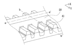
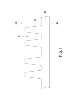
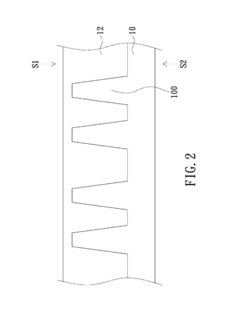
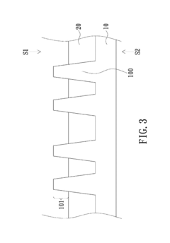
01 FinFET structure design for energy efficiency
Specific structural designs of FinFETs can significantly improve energy efficiency. These designs include optimized fin height-to-width ratios, multi-gate configurations, and novel channel materials. By carefully engineering the physical dimensions and geometry of the fin structure, power consumption can be reduced while maintaining or improving performance characteristics. These structural innovations help address leakage current issues and improve overall energy efficiency in semiconductor devices.- FinFET structure design for energy efficiency: Specific structural designs of FinFETs can significantly improve energy efficiency. These designs include optimized fin dimensions, gate length scaling, and multi-fin configurations that reduce leakage current while maintaining performance. Advanced gate structures and channel engineering techniques help minimize power consumption during operation, making these devices suitable for low-power applications.
- Power reduction techniques in FinFET manufacturing: Various manufacturing techniques can be employed to reduce power consumption in FinFET devices. These include specialized doping profiles, strain engineering, and advanced material selection for the gate stack. Process optimizations during fabrication can lead to devices with lower threshold voltages and improved switching characteristics, resulting in overall energy savings in the final integrated circuits.
- FinFET design optimization through simulation: Computational modeling and simulation tools are crucial for optimizing FinFET designs for energy efficiency. These tools allow for virtual testing of different device parameters and configurations before physical fabrication. Simulation-based approaches help identify optimal device geometries, materials, and operating conditions that minimize power consumption while maintaining required performance metrics.
- Multi-gate FinFET architectures for power efficiency: Advanced multi-gate FinFET architectures offer improved electrostatic control over the channel, leading to better energy efficiency. These designs include double-gate, tri-gate, and gate-all-around structures that provide enhanced control of leakage currents. The improved channel control allows for operation at lower voltages, directly translating to reduced power consumption in digital circuits.
- Integration of FinFETs in low-power circuit applications: FinFET technology can be specifically integrated into circuit designs to minimize overall system power consumption. This includes specialized circuit topologies, power gating techniques, and dynamic voltage scaling methods tailored for FinFET characteristics. The unique properties of FinFETs allow for more efficient implementation of low-power design techniques compared to traditional planar transistors, resulting in energy-efficient integrated circuits for mobile and IoT applications.
02 Low power FinFET circuit techniques
Various circuit design techniques can be implemented to reduce power consumption in FinFET-based systems. These include adaptive voltage scaling, power gating, and clock management strategies specifically optimized for FinFET characteristics. Circuit-level optimizations take advantage of the unique properties of FinFETs to minimize dynamic and static power consumption while maintaining performance requirements. These techniques are particularly important for mobile and battery-powered applications where energy efficiency is critical.Expand Specific Solutions03 Multi-threshold voltage FinFET implementation
Implementing multiple threshold voltage options in FinFET designs allows for optimized power-performance tradeoffs. By using different threshold voltages for different parts of a circuit, designers can allocate higher performance (lower threshold) transistors to critical paths while using higher threshold transistors for non-critical paths to reduce leakage. This approach enables fine-tuned energy efficiency across the entire chip while maintaining overall system performance requirements.Expand Specific Solutions04 FinFET manufacturing processes for energy optimization
Advanced manufacturing processes specifically developed for FinFETs can significantly impact energy consumption. These include specialized doping profiles, strain engineering techniques, and gate stack optimizations that reduce parasitic capacitances and resistances. Process innovations such as high-k metal gates and optimized source/drain engineering help minimize leakage currents and switching energy, resulting in more energy-efficient transistors without compromising performance or reliability.Expand Specific Solutions05 FinFET design automation and simulation for power optimization
Design automation tools and simulation techniques specifically developed for FinFET technology enable power optimization at early design stages. These tools provide accurate power modeling, allowing designers to evaluate energy consumption tradeoffs before manufacturing. Advanced simulation capabilities account for the three-dimensional nature of FinFETs and their unique electrical characteristics, enabling more precise power optimization strategies and reducing the need for costly design iterations.Expand Specific Solutions
Leading Semiconductor Manufacturers in FinFET for IoT
The FinFET technology market for IoT energy optimization is currently in a growth phase, with increasing adoption driven by demands for power-efficient devices. The market is expanding rapidly as IoT deployments accelerate globally, with major semiconductor players competing to deliver energy-optimized solutions. Leading companies like TSMC and GlobalFoundries are at the forefront, leveraging their advanced fabrication capabilities to produce energy-efficient FinFET designs. Qualcomm, NXP, and Infineon are developing specialized IoT chips with optimized power consumption profiles. AMD and IBM contribute significant R&D to advance the technology. The ecosystem shows varying maturity levels, with established players offering commercial solutions while research institutions like Southeast University and CEA focus on next-generation innovations that promise further power efficiency improvements for IoT applications.
Taiwan Semiconductor Manufacturing Co., Ltd.
Technical Solution: TSMC has pioneered advanced FinFET technology specifically optimized for IoT applications through their 12nm and 16nm FinFET Compact Technology (12FFC/16FFC). These processes are tailored for ultra-low power IoT devices, offering up to 50% power reduction compared to previous planar technologies while maintaining performance advantages. TSMC's approach includes multi-threshold voltage options that allow designers to optimize for either performance or power efficiency depending on specific IoT application requirements. Their N12e process technology specifically targets IoT applications, providing an optimal balance of power, performance, and area with reduced leakage current characteristics essential for battery-powered IoT devices. TSMC has also implemented adaptive body biasing techniques in their FinFET designs to dynamically adjust power consumption based on workload demands, extending battery life in IoT deployments[1][3].
Strengths: Industry-leading process node miniaturization with excellent power efficiency metrics; comprehensive design ecosystem supporting IoT-specific optimizations; proven manufacturing reliability at scale. Weaknesses: Higher initial manufacturing costs compared to traditional planar transistors; requires specialized design expertise to fully leverage power optimization features.
GLOBALFOUNDRIES, Inc.
Technical Solution: GlobalFoundries has developed their 22FDX platform specifically addressing IoT energy constraints through FinFET-derived technology. Their approach combines aspects of FinFET architecture with Fully Depleted Silicon-On-Insulator (FD-SOI) technology to create an ultra-low power solution. This platform delivers near-threshold voltage operation capabilities, allowing IoT devices to run at voltages as low as 0.4V, reducing power consumption by up to 70% compared to conventional bulk CMOS processes. GlobalFoundries' technology enables adaptive body biasing, which can dynamically adjust device characteristics to optimize either for performance or power efficiency based on workload requirements. Their platform includes specialized RF integration capabilities essential for IoT connectivity, with built-in RF features that reduce the need for external components, further decreasing overall system power consumption. The company has demonstrated IoT SoCs manufactured on this platform achieving standby power in the nanoWatt range while providing sufficient processing capabilities for edge computing applications[2][5].
Strengths: Excellent ultra-low voltage operation capabilities; superior RF integration for wireless IoT applications; flexible power/performance tuning through body biasing. Weaknesses: Limited to larger process nodes compared to leading-edge FinFET; requires specialized design approaches to fully leverage the FD-SOI advantages.
Key Patents and Innovations in Low-Power FinFET Design
SiGe FINFET WITH IMPROVED JUNCTION DOPING CONTROL
PatentInactiveUS20160172469A1
Innovation
- A method involving the formation of SiGe fins with recessed structures, n-doped silicon layers, and p-doped silicon or SiGe layers, followed by silicide layer formation, to achieve abrupt junctions and reduced access resistance, using techniques like dry plasma etching and epitaxial growth to ensure proper doping and junction formation without ion implantation.


Fin field effect transistor device and fabrication method thereof
PatentActiveUS20160163837A1
Innovation
- A method for fabricating a FinFET device involving the formation of a substrate with a fin structure, an oxide layer, shallow trench isolation, spacers, and an epitaxial fin structure, where the gate structure is perpendicular to the epitaxial fin, and the epitaxial fin can be made of germanium with varying compositions, allowing for improved electrical control and efficiency.
Supply Chain Considerations for IoT FinFET Production
The global supply chain for FinFET production targeting IoT applications presents unique challenges and opportunities that significantly impact energy optimization efforts. Semiconductor manufacturing for advanced FinFET nodes requires sophisticated equipment, rare materials, and specialized expertise, creating a complex ecosystem that spans multiple countries and companies.
Raw material sourcing represents the first critical link in this chain, with high-purity silicon, rare earth elements, and specialty gases being essential components. The geographical concentration of these resources—particularly in regions like China for rare earth elements—introduces geopolitical vulnerabilities that can affect production continuity and ultimately impact energy-optimized designs for IoT applications.
Fabrication capacity for advanced FinFET nodes remains concentrated among a few major players, including TSMC, Samsung, and Intel. This oligopolistic structure creates potential bottlenecks when demand surges, as witnessed during recent global chip shortages. For IoT implementations specifically seeking energy-optimized FinFETs, limited production capacity can force compromises in design or delay market entry for innovative low-power solutions.
The specialized equipment required for FinFET production, particularly extreme ultraviolet (EUV) lithography systems from suppliers like ASML, represents another critical supply chain constraint. With each EUV system costing upwards of $150 million and having limited production capacity, access to these tools directly impacts manufacturers' ability to produce the most energy-efficient FinFET designs at scale.
Testing and packaging operations, often overlooked but essential components of the supply chain, introduce additional complexity. The specialized equipment needed to validate energy performance characteristics of IoT-targeted FinFETs requires continuous calibration and expertise, with much of this capacity concentrated in East Asian manufacturing hubs.
Logistics considerations have gained prominence following recent global disruptions. The semiconductor industry's just-in-time inventory practices proved vulnerable during the COVID-19 pandemic, leading to significant delays in fulfilling orders for energy-optimized chips. This has prompted a reevaluation of inventory management practices specifically for IoT-critical components.
Regionalization trends are reshaping the FinFET supply chain landscape, with major economies investing in domestic semiconductor manufacturing capacity. The CHIPS Act in the US, similar initiatives in Europe, and China's push for semiconductor self-sufficiency will likely create a more distributed but potentially less efficient global production network for energy-optimized FinFETs.
Environmental sustainability considerations are increasingly influencing supply chain decisions, with water usage and energy consumption during manufacturing becoming important factors. The carbon footprint of producing highly energy-efficient IoT chips presents an interesting paradox that manufacturers must address through lifecycle assessment approaches.
Thermal Management Strategies for IoT FinFET Devices
Thermal management has emerged as a critical challenge in FinFET-based IoT devices, particularly as miniaturization continues to increase power density in smaller form factors. The unique three-dimensional structure of FinFETs, while beneficial for performance and leakage control, creates concentrated heat zones that require specialized thermal management approaches. Conventional cooling methods often prove inadequate for IoT applications where device size, power constraints, and environmental conditions present unique challenges.
Advanced materials play a significant role in thermal management strategies for IoT FinFET devices. The integration of high thermal conductivity materials such as diamond-like carbon, graphene, and specialized metal alloys in heat spreaders and thermal interface materials has shown promising results in laboratory settings. These materials facilitate more efficient heat dissipation from the active regions of FinFET structures, preventing localized hotspots that can degrade performance and reliability.
Dynamic thermal management (DTM) techniques represent another crucial approach for IoT implementations. These systems continuously monitor temperature profiles across the device and adjust operating parameters accordingly. Adaptive voltage scaling, frequency throttling, and workload distribution algorithms can be implemented with minimal overhead, making them suitable for resource-constrained IoT applications. Recent research indicates that machine learning-enhanced DTM systems can predict thermal patterns and preemptively adjust parameters before critical thresholds are reached.
3D integration and packaging innovations also contribute significantly to thermal management in IoT FinFET devices. Through-silicon vias (TSVs) and interposer technologies enable more efficient vertical heat transfer paths. Microchannel cooling structures embedded within the packaging can provide targeted cooling to high-temperature regions without significantly increasing device dimensions. These approaches are particularly valuable for edge computing IoT devices that require higher processing capabilities in compact form factors.
For ultra-low-power IoT applications, passive cooling strategies have been refined to address FinFET thermal challenges. Optimized fin geometry and spacing configurations can enhance natural convection cooling without requiring additional power. Phase-change materials incorporated into device packaging provide temperature stabilization during burst processing activities common in many IoT applications, absorbing excess heat during peak operations and releasing it during idle periods.
The environmental conditions in which IoT devices operate present unique thermal management challenges. Devices deployed in outdoor or industrial settings must contend with ambient temperature fluctuations, humidity, and potential exposure to contaminants. Hermetically sealed thermal management solutions with specialized coatings have been developed to maintain optimal operating temperatures while protecting against environmental factors that could compromise device integrity.
Unlock deeper insights with PatSnap Eureka Quick Research — get a full tech report to explore trends and direct your research. Try now!
Generate Your Research Report Instantly with AI Agent
Supercharge your innovation with PatSnap Eureka AI Agent Platform!