

How to Elevate Device Performance with PNP Transistor Integration?
JUL 28, 202510 MIN READ
Generate Your Research Report Instantly with AI Agent
PatSnap Eureka helps you evaluate technical feasibility & market potential.
PNP Transistor Evolution and Integration Goals
The evolution of PNP transistors and their integration into electronic devices has been a cornerstone of semiconductor technology advancement. Since their inception in the mid-20th century, PNP transistors have undergone significant improvements in design, fabrication, and performance. The primary goal of PNP transistor integration has been to enhance device performance while addressing the challenges of power consumption, speed, and miniaturization.
Initially, PNP transistors were developed as a complement to NPN transistors, allowing for more versatile circuit designs. The early germanium-based PNP transistors paved the way for silicon-based devices, which offered improved stability and higher operating temperatures. As the semiconductor industry progressed, the focus shifted towards reducing the size of transistors while increasing their density on integrated circuits.
The introduction of planar technology in the 1960s marked a significant milestone in PNP transistor evolution. This innovation allowed for more precise control over the transistor's structure and enabled mass production of integrated circuits. Subsequently, the development of epitaxial growth techniques further improved the performance and reliability of PNP transistors.
In recent decades, the integration goals for PNP transistors have aligned closely with Moore's Law, aiming to double the number of transistors on a chip every two years. This drive for miniaturization has led to the development of advanced manufacturing processes, such as deep submicron and nanometer-scale fabrication techniques. These advancements have not only reduced the size of PNP transistors but also improved their switching speeds and power efficiency.
The current integration goals for PNP transistors focus on overcoming the physical limitations of traditional silicon-based devices. Researchers and engineers are exploring novel materials and structures to push the boundaries of transistor performance. For instance, the use of III-V compound semiconductors and silicon-germanium alloys has shown promise in enhancing carrier mobility and reducing power consumption in PNP transistors.
Another critical objective in PNP transistor integration is to address the increasing demand for low-power, high-performance devices in mobile and IoT applications. This has led to the development of advanced PNP transistor designs that offer better control over leakage currents and improved thermal characteristics. Additionally, the integration of PNP transistors with complementary metal-oxide-semiconductor (CMOS) technology has become crucial for creating more efficient and versatile integrated circuits.
Looking ahead, the future goals of PNP transistor integration include exploring three-dimensional architectures, such as FinFETs and gate-all-around transistors, to further enhance performance and density. Additionally, research into quantum effects and novel switching mechanisms aims to overcome the fundamental limits of classical transistor scaling. These efforts are essential for continuing the trajectory of device performance improvement and enabling the next generation of electronic systems.
Market Demand for Enhanced Device Performance
The market demand for enhanced device performance has been steadily increasing across various sectors, driven by the need for more efficient and powerful electronic systems. PNP transistor integration plays a crucial role in meeting these demands, offering significant improvements in device capabilities and overall system performance.
In the consumer electronics sector, there is a growing appetite for devices with longer battery life, faster processing speeds, and improved multitasking capabilities. Smartphones, tablets, and laptops are at the forefront of this demand, with consumers expecting seamless performance even when running multiple applications simultaneously. The integration of PNP transistors can address these needs by enabling more efficient power management and enhanced signal processing.
The automotive industry is another key driver of demand for improved device performance. As vehicles become increasingly electrified and autonomous, the need for advanced electronic systems with higher reliability and efficiency has surged. PNP transistor integration can contribute to the development of more sophisticated engine control units, advanced driver assistance systems, and infotainment systems, all of which require superior performance and power efficiency.
In the industrial sector, the rise of Industry 4.0 and the Internet of Things (IoT) has created a substantial demand for high-performance devices capable of real-time data processing and analysis. Factory automation, smart sensors, and industrial control systems all benefit from the enhanced capabilities offered by PNP transistor integration, enabling more precise control, faster response times, and improved energy efficiency.
The telecommunications industry is experiencing a significant shift with the rollout of 5G networks, driving demand for devices that can handle higher data rates and lower latency. Base stations, network switches, and mobile devices all require improved performance to fully leverage the capabilities of 5G technology. PNP transistor integration can contribute to the development of more efficient and powerful communication equipment, supporting the expansion of 5G infrastructure.
In the healthcare sector, there is a growing need for advanced medical devices with improved performance and reliability. From diagnostic equipment to implantable devices, the integration of PNP transistors can enhance the accuracy, speed, and energy efficiency of these critical systems, ultimately leading to better patient outcomes and more effective healthcare delivery.
The demand for enhanced device performance extends to the aerospace and defense sectors as well. These industries require highly reliable and robust electronic systems capable of operating in extreme conditions. PNP transistor integration can contribute to the development of more advanced avionics, radar systems, and communication equipment, meeting the stringent performance requirements of these applications.
As the global focus on sustainability and energy efficiency intensifies, there is an increasing demand for devices that can deliver higher performance while consuming less power. PNP transistor integration aligns well with this trend, offering the potential for significant improvements in energy efficiency across a wide range of applications, from consumer electronics to industrial systems.
Current PNP Integration Challenges
The integration of PNP transistors into modern semiconductor devices presents several significant challenges that hinder the optimization of device performance. One of the primary obstacles is the inherent slower switching speed of PNP transistors compared to their NPN counterparts. This speed limitation is due to the lower mobility of holes, which are the majority carriers in PNP devices, compared to electrons in NPN transistors. As a result, designers must carefully balance the use of PNP transistors to avoid compromising overall circuit speed and efficiency.
Another critical challenge lies in the thermal management of PNP transistors. These devices tend to generate more heat during operation, which can lead to performance degradation and reliability issues if not properly addressed. The increased heat generation is partly due to the higher resistance of the P-type material and the larger voltage drops across PNP junctions. Consequently, integrating effective cooling solutions and implementing robust thermal design practices become crucial considerations in PNP transistor integration.
The fabrication process for PNP transistors also presents unique challenges. Achieving precise doping profiles and maintaining consistent electrical characteristics across large-scale production can be more difficult with PNP structures. This is particularly evident in vertical PNP transistors, where the collector region is typically formed in the substrate, limiting the flexibility of device design and potentially impacting performance metrics such as current gain and breakdown voltage.
Furthermore, the integration of PNP transistors in complementary bipolar and BiCMOS processes introduces additional complexities. Balancing the performance characteristics of both NPN and PNP devices within the same process flow requires careful optimization of fabrication steps, often leading to trade-offs in device parameters. This challenge is exacerbated in high-frequency applications, where the inherent limitations of PNP transistors become more pronounced.
The scaling of PNP transistors to smaller geometries also presents significant hurdles. As device dimensions shrink, maintaining adequate current gain and managing parasitic effects become increasingly difficult. The reduced base width in scaled PNP devices can lead to increased base resistance and potential punch-through effects, compromising device reliability and performance consistency across different operating conditions.
Lastly, the integration of PNP transistors in modern power management circuits poses unique challenges. While PNP devices are essential for certain power control functions, their higher on-resistance and slower switching characteristics can limit the efficiency of power conversion and regulation circuits. Designers must carefully consider these limitations when implementing PNP transistors in high-efficiency power management solutions, often requiring innovative circuit topologies and control strategies to mitigate their inherent drawbacks.
Existing PNP Integration Techniques
01 Fabrication techniques for PNP transistors
Various fabrication techniques are employed to enhance PNP transistor performance. These include optimizing doping profiles, improving epitaxial growth processes, and refining ion implantation methods. Advanced lithography and etching techniques are also used to achieve precise control over transistor dimensions and reduce parasitic capacitances.- Fabrication techniques for improved PNP transistor performance: Various fabrication techniques are employed to enhance PNP transistor performance. These include optimizing doping profiles, improving junction formation, and refining epitaxial growth processes. Advanced lithography and etching methods are also used to achieve better control over transistor dimensions and reduce parasitic effects.
- Circuit design strategies for PNP transistor optimization: Circuit designers employ various strategies to optimize PNP transistor performance in integrated circuits. These include careful biasing techniques, load selection, and feedback mechanisms. Advanced circuit topologies are developed to mitigate limitations of PNP transistors and exploit their unique characteristics.
- Structural modifications for enhanced PNP transistor characteristics: Structural modifications are implemented to improve PNP transistor characteristics. These include optimizing base width, emitter geometry, and collector design. Novel device architectures, such as vertical PNP structures or silicon-on-insulator (SOI) configurations, are explored to enhance performance metrics like current gain and frequency response.
- Material innovations for PNP transistor performance enhancement: Advanced materials are investigated to improve PNP transistor performance. This includes exploring alternative semiconductor materials, novel dopants, and advanced contact metallization. Researchers also investigate the use of strained silicon or SiGe alloys in the base region to enhance carrier mobility and overall transistor performance.
- Packaging and thermal management for PNP transistor optimization: Packaging and thermal management techniques are crucial for optimizing PNP transistor performance in practical applications. This involves developing advanced heat dissipation methods, implementing efficient die attach techniques, and designing packages that minimize parasitic effects. Thermal simulation and modeling are used to predict and improve transistor behavior under various operating conditions.
02 Structural improvements in PNP transistors
Structural enhancements play a crucial role in improving PNP transistor performance. These include the development of vertical and lateral PNP structures, implementation of shallow and deep trench isolation, and the use of SiGe bases. Advanced contact and metallization schemes are also employed to reduce parasitic resistances and improve high-frequency performance.Expand Specific Solutions03 Circuit design techniques for PNP transistors
Circuit design techniques are utilized to optimize PNP transistor performance in various applications. These include the development of current mirrors, differential amplifiers, and voltage regulators specifically tailored for PNP transistors. Biasing techniques and feedback mechanisms are also employed to improve linearity and reduce distortion in analog circuits using PNP transistors.Expand Specific Solutions04 Packaging and thermal management for PNP transistors
Packaging and thermal management solutions are crucial for maintaining optimal PNP transistor performance. Advanced packaging techniques, such as flip-chip and wafer-level packaging, are used to minimize parasitic effects and improve heat dissipation. Thermal management strategies, including the use of heat spreaders and advanced cooling solutions, are implemented to maintain stable operating temperatures and prevent performance degradation.Expand Specific Solutions05 Characterization and modeling of PNP transistors
Accurate characterization and modeling techniques are essential for predicting and optimizing PNP transistor performance. Advanced measurement methods, including high-frequency S-parameter extraction and noise figure measurements, are used to characterize PNP transistors. Sophisticated compact models and simulation tools are developed to accurately predict PNP transistor behavior in various operating conditions and circuit configurations.Expand Specific Solutions
Key Players in PNP Transistor Development
The integration of PNP transistors to enhance device performance is at a mature stage in the semiconductor industry, with a substantial market size driven by widespread applications in electronics. Major players like IBM, Infineon Technologies, and GlobalFoundries have established strong positions in this field. The technology's maturity is evident from its adoption by diverse companies, including Texas Instruments, Samsung Electronics, and Qualcomm, who leverage PNP transistors in various products. Research institutions such as the University of Electronic Science & Technology of China and Southeast University continue to contribute to advancements, indicating ongoing innovation despite the technology's established nature.
International Business Machines Corp.
Technical Solution: IBM has developed advanced PNP transistor integration techniques to elevate device performance. Their approach involves using Silicon-Germanium (SiGe) heterojunction bipolar transistors (HBTs) in their BiCMOS technology. This allows for higher current gain, improved frequency response, and lower noise compared to traditional silicon-only transistors[1]. IBM's PNP transistors feature a self-aligned emitter-base structure and optimized doping profiles, resulting in reduced parasitic capacitances and enhanced switching speeds[2]. The company has also implemented vertical PNP structures with buried subcollectors, enabling better isolation and reduced substrate coupling[3]. These innovations have led to PNP transistors with cutoff frequencies exceeding 300 GHz, making them suitable for high-speed analog and mixed-signal applications[4].
Strengths: Superior high-frequency performance, reduced noise, and improved current gain. Ideal for RF and high-speed mixed-signal circuits. Weaknesses: Potentially higher manufacturing costs and complexity compared to standard CMOS processes.
Infineon Technologies AG
Technical Solution: Infineon has focused on integrating high-performance PNP transistors in their power management and automotive semiconductor solutions. Their approach involves using advanced trench isolation techniques and optimized epitaxial layer structures to enhance PNP transistor performance[5]. Infineon's PNP transistors feature reduced collector resistance and improved current handling capabilities, making them suitable for high-power applications[6]. The company has also developed complementary NPN-PNP pairs with closely matched characteristics, enabling precise analog circuit designs[7]. Infineon's PNP integration strategy includes the use of SiGe in the base region for selected high-performance applications, resulting in transistors with higher current gain and improved temperature stability[8].
Strengths: Excellent power handling capabilities, good matching in complementary pairs, and improved temperature stability. Ideal for automotive and industrial applications. Weaknesses: May have limitations in ultra-high-frequency applications compared to some competitors.
Innovative PNP Transistor Designs
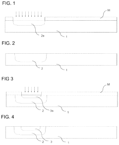
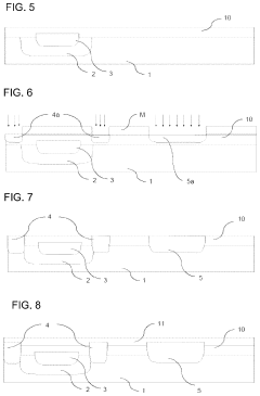
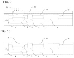
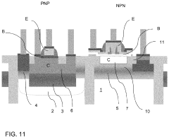
Device comprising a PNP bipolar transistor and NPN bipolar transistor for radiofrequency applications
PatentActiveUS11955481B2
Innovation
- A method involving the formation of two epitaxial semiconductor layers allows burying the P+ well deeper in the substrate without high-energy implantation, optimizing the performance of both PNP and NPN transistors by controlling the thickness and doping of these layers to prevent crystalline defects and enhance transistor speed.
High performance integrated vertical transistors and method of making the same
PatentInactiveUS20070001264A1
Innovation
- The use of a shared silicon germanium (SiGe) low temperature epitaxial (LTE) layer allows for the fabrication of vertically aligned complementary bipolar transistors, where the NPN and PNP transistors share the same epitaxial base and collector regions, with the PNP emitter layer acting as the NPN base layer, utilizing advanced epitaxial techniques like molecular beam epitaxy (MBE) and low temperature epitaxy (LTE) to ensure identical vertical profiles.
Power Efficiency Considerations
Power efficiency is a critical consideration in the integration of PNP transistors to elevate device performance. The inherent characteristics of PNP transistors, such as lower carrier mobility compared to their NPN counterparts, present unique challenges in optimizing power consumption. However, strategic implementation can lead to significant improvements in overall device efficiency.
One key aspect of power efficiency in PNP transistor integration is the reduction of static power dissipation. By carefully designing the transistor's geometry and doping profiles, leakage currents can be minimized, resulting in lower standby power consumption. This is particularly crucial in battery-powered devices where extending operational life is paramount.
Dynamic power consumption, which occurs during transistor switching, also plays a vital role in overall efficiency. PNP transistors typically exhibit slower switching speeds than NPN transistors, potentially leading to increased power dissipation during transitions. To mitigate this, advanced circuit design techniques such as charge recycling and adaptive biasing can be employed to optimize switching behavior and reduce dynamic power losses.
Thermal management is another essential factor in power efficiency considerations. PNP transistors generate heat during operation, which can impact device performance and reliability. Implementing effective heat dissipation strategies, such as optimized layout designs and the use of thermally conductive materials, can help maintain optimal operating temperatures and prevent efficiency degradation due to thermal effects.
The integration of PNP transistors in complementary circuits, such as CMOS configurations, offers opportunities for enhanced power efficiency. By leveraging the complementary nature of PNP and NPN transistors, designers can create circuits that consume minimal power in steady-state conditions while maintaining high performance during active operation. This approach is particularly beneficial in low-power applications where energy conservation is critical.
Advanced process technologies and materials can further contribute to power efficiency improvements in PNP transistor integration. For instance, the use of silicon-germanium (SiGe) or III-V compound semiconductors can enhance carrier mobility and reduce operating voltages, leading to lower power consumption without sacrificing performance. Additionally, the implementation of advanced isolation techniques can minimize parasitic capacitances and leakage paths, further optimizing power efficiency.
In conclusion, elevating device performance through PNP transistor integration requires a multifaceted approach to power efficiency. By addressing static and dynamic power consumption, implementing effective thermal management strategies, leveraging complementary circuit designs, and adopting advanced materials and process technologies, significant improvements in overall device efficiency can be achieved. These considerations are crucial for developing high-performance, energy-efficient electronic devices that meet the demands of modern applications.
Thermal Management Strategies
Thermal management is a critical aspect of integrating PNP transistors to elevate device performance. As power density increases in modern electronic devices, effective heat dissipation becomes paramount to maintain optimal functionality and reliability. PNP transistors, while offering advantages in certain circuit configurations, also contribute to heat generation within the device.
To address thermal challenges, several strategies can be employed. One approach is the implementation of advanced packaging techniques. These may include the use of thermally conductive materials in the transistor package, such as ceramic or metal-core substrates, which facilitate better heat transfer from the transistor junction to the external environment. Additionally, the incorporation of heat spreaders or heat sinks directly integrated into the package can significantly enhance thermal dissipation capabilities.
Another effective strategy involves optimizing the circuit layout and component placement. By strategically positioning PNP transistors and other heat-generating components, designers can create thermal pathways that efficiently channel heat away from critical areas. This may involve the use of thermal vias, which are specialized through-hole connections designed to conduct heat vertically through PCB layers, improving overall thermal management.
Active cooling solutions also play a crucial role in managing heat generated by PNP transistors. Miniature fans or blowers can be integrated into the device design to provide forced air cooling, particularly effective for localized hot spots. For more demanding applications, thermoelectric coolers (TECs) or liquid cooling systems may be employed to achieve precise temperature control and heat removal.
At the semiconductor level, advancements in transistor design and fabrication processes can contribute to improved thermal performance. Techniques such as silicon-on-insulator (SOI) technology or the use of high-bandgap materials can help reduce leakage currents and improve the overall efficiency of PNP transistors, thereby minimizing heat generation at the source.
Furthermore, the implementation of intelligent thermal management systems can dynamically adjust device performance based on temperature feedback. This may involve the use of integrated temperature sensors and control algorithms that modulate transistor operation or system clock speeds to maintain optimal thermal conditions under varying workloads.
By combining these thermal management strategies, designers can effectively mitigate the heat-related challenges associated with PNP transistor integration, ultimately enabling enhanced device performance and reliability. The selection and implementation of specific thermal solutions should be tailored to the unique requirements of each application, considering factors such as power consumption, form factor constraints, and environmental conditions.
Unlock deeper insights with PatSnap Eureka Quick Research — get a full tech report to explore trends and direct your research. Try now!
Generate Your Research Report Instantly with AI Agent
Supercharge your innovation with PatSnap Eureka AI Agent Platform!