

PNP Transistors: A Catalyst in Transformative Tech Evolution
JUL 28, 20259 MIN READ
Generate Your Research Report Instantly with AI Agent
PatSnap Eureka helps you evaluate technical feasibility & market potential.
PNP Transistor Evolution
The evolution of PNP transistors has been a cornerstone in the transformative journey of electronic technology. Since their inception in the early 1950s, these devices have undergone significant advancements, shaping the landscape of modern electronics.
In the initial stages, PNP transistors were primarily germanium-based, offering limited performance and reliability. The 1960s marked a pivotal shift with the introduction of silicon-based PNP transistors, which demonstrated superior characteristics in terms of temperature stability and overall performance. This transition laid the foundation for more robust and versatile electronic applications.
The 1970s and 1980s witnessed remarkable progress in PNP transistor technology. Manufacturers focused on miniaturization and improved manufacturing processes, leading to the development of high-frequency PNP transistors. These advancements enabled the creation of more compact and efficient electronic devices, paving the way for portable consumer electronics.
The 1990s brought about a revolution in PNP transistor design with the introduction of complementary bipolar processes. This innovation allowed for the integration of both PNP and NPN transistors on the same chip, significantly enhancing the functionality and performance of integrated circuits. The ability to combine different transistor types opened new possibilities in analog and mixed-signal circuit design.
As we entered the 21st century, the focus shifted towards optimizing PNP transistors for specific applications. High-power PNP transistors found their niche in automotive and industrial sectors, while low-noise PNP transistors became crucial components in sensitive audio and communication equipment. The continuous refinement of manufacturing techniques led to the production of PNP transistors with improved current gain, reduced parasitic capacitance, and enhanced frequency response.
Recent years have seen a renewed interest in PNP transistors within the context of emerging technologies. The rise of Internet of Things (IoT) devices and wearable technology has driven demand for ultra-low-power PNP transistors capable of operating efficiently in battery-powered applications. Additionally, advancements in compound semiconductor materials have opened new avenues for high-performance PNP transistors in specialized applications such as high-frequency communications and power electronics.
Looking ahead, the evolution of PNP transistors is expected to continue, with a focus on further miniaturization, increased energy efficiency, and integration with novel materials and structures. The development of vertical PNP transistors and the exploration of new semiconductor compounds promise to extend the capabilities of these devices, ensuring their relevance in the next generation of electronic systems.
Market Demand Analysis
The market demand for PNP transistors continues to grow steadily, driven by the increasing complexity and miniaturization of electronic devices across various industries. As a fundamental component in analog and mixed-signal circuits, PNP transistors play a crucial role in amplification, switching, and signal processing applications.
In the consumer electronics sector, the demand for PNP transistors is particularly strong. The proliferation of smartphones, tablets, and wearable devices has created a significant market for high-performance, low-power transistors. PNP transistors are essential in power management circuits, audio amplifiers, and battery charging systems, contributing to improved energy efficiency and extended battery life in portable devices.
The automotive industry represents another major market for PNP transistors. With the rapid advancement of electric and hybrid vehicles, there is an increasing need for sophisticated power management and control systems. PNP transistors are utilized in motor control circuits, battery management systems, and various sensor interfaces, supporting the transition towards more electrified and autonomous vehicles.
In the industrial sector, PNP transistors find applications in automation systems, process control equipment, and power supplies. The ongoing trend of Industry 4.0 and the Industrial Internet of Things (IIoT) is driving demand for smart sensors and actuators, many of which incorporate PNP transistors in their signal conditioning and interface circuits.
The telecommunications industry also contributes significantly to the market demand for PNP transistors. As 5G networks continue to expand globally, there is a growing need for high-frequency, low-noise transistors in base station equipment and mobile devices. PNP transistors are used in RF amplifiers, mixers, and other critical components of wireless communication systems.
The medical electronics sector presents a promising growth area for PNP transistors. Advanced medical devices, such as implantable sensors, wearable health monitors, and portable diagnostic equipment, rely on PNP transistors for their compact size, low power consumption, and reliable performance in analog signal processing.
Market analysts project that the global transistor market, including PNP transistors, will experience steady growth in the coming years. This growth is attributed to the increasing adoption of IoT devices, the expansion of 5G networks, and the continued electrification of various industries. The demand for high-performance, energy-efficient transistors is expected to drive innovation in PNP transistor design and manufacturing processes.
Technical Challenges
PNP transistors, while fundamental to modern electronics, face several technical challenges that hinder their widespread adoption and limit their performance in certain applications. One of the primary issues is the inherent slower switching speed compared to their NPN counterparts. This speed limitation is due to the mobility of holes, which are the majority carriers in PNP transistors, being lower than that of electrons in NPN transistors.
Another significant challenge is the higher power consumption of PNP transistors. The larger base current required for operation results in increased power dissipation, making them less suitable for low-power applications and portable devices where energy efficiency is crucial. This power inefficiency also contributes to heat generation, which can affect the overall performance and reliability of the device.
The manufacturing process for PNP transistors presents its own set of challenges. The fabrication of high-quality PNP transistors often requires more complex and costly production techniques compared to NPN transistors. This complexity can lead to increased variability in device characteristics and potentially lower yields in manufacturing.
Noise performance is another area where PNP transistors face difficulties. They tend to exhibit higher noise levels, particularly at low frequencies, which can be problematic in sensitive analog circuits and precision measurement applications. This noise issue limits their use in high-fidelity audio equipment and certain types of sensors.
Temperature sensitivity is a further concern for PNP transistors. Their performance can vary significantly with temperature changes, affecting the stability and reliability of circuits in which they are used. This temperature dependence necessitates additional compensation mechanisms in many applications, adding to design complexity.
The voltage handling capability of PNP transistors is generally lower than that of NPN transistors, limiting their use in high-voltage applications. This restriction narrows the range of potential applications and requires careful consideration in circuit design to ensure safe and reliable operation.
Lastly, the integration of PNP transistors in modern semiconductor processes, particularly in CMOS technology, presents ongoing challenges. While vertical PNP transistors are commonly available in bipolar and BiCMOS processes, lateral PNP transistors in standard CMOS processes often suffer from poor performance characteristics, limiting their utility in mixed-signal integrated circuits.
Current PNP Solutions
01 Structure and fabrication of PNP transistors
PNP transistors are semiconductor devices with specific structures and fabrication methods. They typically consist of a p-type emitter, n-type base, and p-type collector. The manufacturing process involves various steps such as doping, etching, and layering to create the desired transistor characteristics.- PNP transistor structure and fabrication: This category focuses on the physical structure and manufacturing processes of PNP transistors. It includes innovations in the design of the emitter, base, and collector regions, as well as techniques for doping and layering semiconductor materials to create efficient PNP devices.
- PNP transistor applications in integrated circuits: This point covers the use of PNP transistors in various integrated circuit designs. It includes their implementation in analog and digital circuits, power management systems, and specialized applications such as memory devices or signal processing units.
- PNP transistor performance optimization: This category deals with methods and techniques to enhance the performance of PNP transistors. It includes strategies for improving current gain, reducing noise, increasing switching speed, and enhancing overall efficiency of the device.
- PNP transistors in power electronics: This point focuses on the use of PNP transistors in power electronic applications. It covers their implementation in high-voltage and high-current circuits, power amplifiers, voltage regulators, and other power management systems.
- PNP transistor testing and characterization: This category encompasses methods and systems for testing and characterizing PNP transistors. It includes techniques for measuring key parameters, analyzing performance under various conditions, and ensuring quality control in manufacturing processes.
02 Applications of PNP transistors in electronic circuits
PNP transistors are widely used in various electronic circuits for amplification, switching, and signal processing. They are essential components in analog and digital circuits, including power supplies, audio amplifiers, and logic gates. Their unique properties make them suitable for specific circuit designs and applications.Expand Specific Solutions03 Integration of PNP transistors in semiconductor devices
PNP transistors are often integrated into larger semiconductor devices and integrated circuits. This integration allows for the creation of complex electronic systems on a single chip, improving performance and reducing size. Various techniques are used to optimize the integration process and enhance overall device functionality.Expand Specific Solutions04 Performance optimization and characterization of PNP transistors
Improving the performance of PNP transistors involves optimizing various parameters such as gain, frequency response, and power handling capabilities. Characterization techniques are used to measure and analyze transistor properties, enabling engineers to fine-tune designs for specific applications and requirements.Expand Specific Solutions05 Novel designs and materials for PNP transistors
Research and development efforts focus on creating novel PNP transistor designs and exploring new materials to enhance performance and functionality. These innovations aim to improve factors such as speed, power efficiency, and thermal stability, pushing the boundaries of transistor technology.Expand Specific Solutions
Key Industry Players
The PNP transistor market is in a mature stage, with established players dominating the industry. The global market size for PNP transistors is substantial, driven by their widespread use in various electronic applications. Technologically, PNP transistors are well-developed, with companies like International Business Machines Corp., QUALCOMM, Inc., and Samsung Electronics Co., Ltd. continuously innovating to improve performance and efficiency. These industry leaders, along with other key players such as Infineon Technologies AG and STMicroelectronics, are focusing on miniaturization, power efficiency, and integration with advanced semiconductor technologies to maintain their competitive edge in this transformative tech evolution.
International Business Machines Corp.
Technical Solution: IBM has been at the forefront of PNP transistor technology development, particularly in the field of silicon-germanium (SiGe) heterojunction bipolar transistors (HBTs). Their advanced PNP transistors have achieved record-breaking performance, with cut-off frequencies exceeding 350 GHz [1]. IBM's approach involves optimizing the base and emitter regions of the transistor structure, utilizing advanced epitaxial growth techniques to create precise dopant profiles and reduce parasitic capacitances [2]. The company has also developed innovative collector designs that minimize transit times, further enhancing the transistor's speed capabilities [3].
Strengths: Unparalleled high-frequency performance, ideal for RF and mm-wave applications. Weaknesses: Complex manufacturing process may lead to higher production costs compared to standard bipolar transistors.
QUALCOMM, Inc.
Technical Solution: Qualcomm has made significant strides in PNP transistor technology, focusing on their integration into advanced mobile and wireless communication systems. Their approach involves developing complementary bipolar-CMOS (BiCMOS) processes that incorporate high-performance PNP transistors alongside CMOS logic [4]. Qualcomm's PNP transistors feature optimized vertical profiles and lateral scaling to achieve high current gain and low parasitic capacitances. The company has also implemented innovative emitter and collector contact designs to reduce series resistance and improve high-frequency performance [5]. These advancements have enabled Qualcomm to produce PNP transistors with ft values exceeding 200 GHz, suitable for 5G and beyond applications [6].
Strengths: Excellent integration with CMOS technology, enabling highly integrated RF front-end modules. Weaknesses: May have slightly lower absolute performance compared to dedicated bipolar processes.
Core PNP Innovations
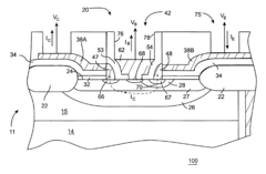
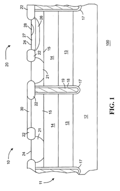
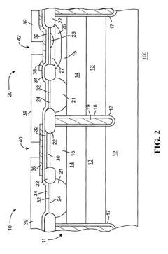
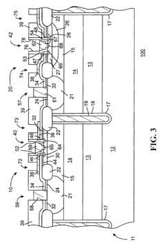
Integrated circuit with a high speed narrow base width vertical PNP transistor
PatentInactiveUS6809396B2
Innovation
- A semiconductor device is fabricated with both high-performance NPN and PNP vertical transistors on a monocrystalline silicon substrate, utilizing a heavily doped base layer, epitaxial layers, and buried layers to reduce parasitic capacitance and collector resistance, along with trench isolation and tailored doping profiles to achieve low manufacturing costs and high frequency response.
Integration of bipolar device and backside power delivery network
PatentPendingUS20250192049A1
Innovation
- A semiconductor device is developed that integrates BJTs with direct backside contact and accurate backside contact depth control, enabling the formation of a power delivery network (PSPDN) for bipolar devices co-integrated with logic devices.


PNP Manufacturing Process
The manufacturing process of PNP transistors is a critical aspect of semiconductor production, involving several intricate steps to create these essential electronic components. The process begins with the selection of a high-quality silicon wafer, which serves as the substrate for the transistor. This wafer undergoes a series of precise treatments to prepare it for the subsequent stages of fabrication.
The first major step in PNP transistor manufacturing is the creation of the N-type collector region. This is typically achieved through epitaxial growth, where a thin layer of N-type semiconductor material is deposited onto the P-type substrate. The epitaxial process allows for precise control over the thickness and doping concentration of the collector region, which is crucial for the transistor's performance characteristics.
Following the formation of the collector, the base region is created through a process called ion implantation. In this step, P-type dopants are selectively introduced into the N-type collector layer to form the base. The ion implantation process allows for precise control over the depth and concentration of the dopants, enabling the creation of very thin base regions essential for high-frequency performance.
The emitter region, which is the final active area of the PNP transistor, is then formed. This is typically done through a combination of photolithography and diffusion processes. A mask is applied to the surface of the wafer, and P-type dopants are diffused into the exposed areas to create the emitter region. The diffusion process is carefully controlled to ensure the proper depth and concentration of dopants.
After the formation of the three primary regions (collector, base, and emitter), the wafer undergoes several additional processing steps. These include the deposition of insulating layers, the creation of contact windows, and the metallization process to form electrical connections to the transistor's regions. The metallization step is particularly critical, as it involves depositing and patterning metal layers to create the electrodes that will connect the transistor to external circuitry.
The final stages of PNP transistor manufacturing involve passivation, where a protective layer is applied to the surface of the device to prevent contamination and improve reliability. The wafer is then diced into individual transistor chips, which are packaged and tested before being integrated into electronic circuits.
Throughout the manufacturing process, strict quality control measures are implemented to ensure the consistency and reliability of the produced transistors. Advanced metrology and inspection techniques are employed at various stages to monitor critical parameters such as layer thicknesses, doping profiles, and electrical characteristics. This rigorous approach to manufacturing has enabled the continuous improvement of PNP transistor performance and reliability, contributing to their widespread use in modern electronic systems.
Environmental Impact
The environmental impact of PNP transistors and their role in transformative tech evolution is a multifaceted issue that warrants careful consideration. These semiconductor devices have played a significant role in the miniaturization and increased efficiency of electronic systems, contributing to reduced energy consumption in various applications. As electronic devices become more compact and energy-efficient, the overall carbon footprint associated with their production and operation has decreased.
However, the manufacturing process of PNP transistors, like other semiconductor components, involves the use of various chemicals and materials that can have environmental implications. The production of high-purity silicon, essential for transistor fabrication, requires substantial energy input and can generate waste products. Additionally, the etching and doping processes used in transistor manufacturing often involve hazardous chemicals that need careful handling and disposal to prevent environmental contamination.
On the positive side, the widespread adoption of PNP transistors in power management circuits has led to more efficient energy utilization in electronic devices. This improved efficiency translates to longer battery life in portable devices and reduced power consumption in larger systems, ultimately contributing to energy conservation on a global scale. The role of PNP transistors in enabling more sophisticated control systems has also facilitated the development of smart grids and energy management systems, further enhancing overall energy efficiency.
The miniaturization trend driven by advancements in transistor technology, including PNP transistors, has led to a reduction in the amount of raw materials required for electronic device production. This not only conserves resources but also minimizes the environmental impact associated with mining and processing these materials. Furthermore, the increased functionality and longevity of modern electronic devices, partly attributable to improved transistor technology, has the potential to reduce electronic waste generation.
Nevertheless, the rapid pace of technological advancement and the resulting obsolescence of electronic devices present challenges in terms of e-waste management. While PNP transistors themselves are not typically the primary concern in e-waste, they are integral components of countless electronic products that eventually become obsolete. Proper recycling and disposal of these devices are crucial to mitigate potential environmental hazards associated with heavy metals and other harmful substances present in electronic components.
In conclusion, while PNP transistors have contributed significantly to technological progress and energy efficiency, their environmental impact is a complex issue that requires ongoing attention and innovation in manufacturing processes, device design, and end-of-life management to ensure a sustainable technological future.
Unlock deeper insights with PatSnap Eureka Quick Research — get a full tech report to explore trends and direct your research. Try now!
Generate Your Research Report Instantly with AI Agent
Supercharge your innovation with PatSnap Eureka AI Agent Platform!