

Exploring Breakthroughs in PNP Transistor Architectural Design
JUL 28, 202510 MIN READ
Generate Your Research Report Instantly with AI Agent
Patsnap Eureka helps you evaluate technical feasibility & market potential.
PNP Transistor Evolution and Design Goals
The evolution of PNP transistor architecture has been a cornerstone in the advancement of semiconductor technology since its inception in the mid-20th century. Initially developed as a complement to NPN transistors, PNP transistors have undergone significant transformations in design and functionality. The journey began with germanium-based devices, which were soon superseded by silicon-based transistors due to their superior performance characteristics and manufacturability.
Throughout the decades, PNP transistor design has been driven by the relentless pursuit of miniaturization, improved efficiency, and enhanced performance. The transition from bipolar junction transistors (BJTs) to field-effect transistors (FETs) marked a pivotal moment in this evolution, enabling lower power consumption and higher integration densities. The introduction of complementary metal-oxide-semiconductor (CMOS) technology further revolutionized the field, allowing for the creation of more complex and energy-efficient integrated circuits.
Recent advancements in PNP transistor architecture have focused on overcoming the limitations imposed by traditional planar designs. The development of three-dimensional structures, such as FinFETs and gate-all-around (GAA) transistors, has opened new avenues for performance optimization. These innovative architectures offer better electrostatic control, reduced short-channel effects, and improved current drive capabilities.
The primary goals driving the exploration of breakthroughs in PNP transistor architectural design are multifaceted. Firstly, there is a continuous push for further miniaturization to accommodate the increasing demand for more transistors per chip, as predicted by Moore's Law. This necessitates novel approaches to overcome the physical limitations of traditional scaling techniques.
Secondly, power efficiency remains a critical objective, particularly in the context of mobile and IoT devices where battery life is paramount. Researchers are exploring new materials and structures that can minimize leakage currents and reduce overall power consumption without compromising performance.
Another key goal is to enhance the switching speed and frequency response of PNP transistors, enabling their use in high-frequency applications such as 5G and beyond. This involves optimizing the carrier mobility and reducing parasitic capacitances through innovative design strategies.
Furthermore, the integration of PNP transistors with emerging technologies, such as spintronics and quantum computing, presents exciting opportunities for future breakthroughs. These interdisciplinary approaches aim to leverage quantum mechanical properties to create transistors with unprecedented capabilities.
Lastly, the quest for more robust and reliable PNP transistor designs continues, with a focus on improving thermal management, radiation hardness, and overall device longevity. These enhancements are crucial for applications in harsh environments and mission-critical systems.
Market Demand Analysis for Advanced PNP Transistors
The market demand for advanced PNP transistors has been steadily increasing, driven by the growing need for high-performance electronic devices across various industries. As consumer electronics, automotive systems, and industrial applications continue to evolve, there is a rising demand for transistors that can deliver improved efficiency, reduced power consumption, and enhanced thermal management.
In the consumer electronics sector, the push for smaller, more powerful devices has created a significant market opportunity for advanced PNP transistors. Smartphones, tablets, and wearable technologies require compact transistors that can handle high currents while maintaining low power dissipation. This trend is expected to continue, with the global smartphone market projected to reach 1.5 billion units by 2025.
The automotive industry represents another major growth area for advanced PNP transistors. With the increasing adoption of electric and hybrid vehicles, there is a surging demand for high-voltage, high-current transistors capable of managing power distribution efficiently. The global electric vehicle market is forecasted to grow at a CAGR of 29% from 2021 to 2026, further driving the need for advanced transistor technologies.
Industrial automation and control systems also contribute significantly to the market demand for advanced PNP transistors. These applications require robust, reliable transistors that can operate in harsh environments and handle high-frequency switching. The industrial automation market is expected to reach $306 billion by 2027, indicating substantial growth potential for transistor manufacturers.
The telecommunications sector, particularly with the ongoing rollout of 5G networks, presents another key market for advanced PNP transistors. Base stations and network infrastructure equipment demand high-performance transistors capable of operating at higher frequencies and power levels. The global 5G infrastructure market is projected to grow at a CAGR of 49% from 2021 to 2027.
Emerging technologies such as artificial intelligence, Internet of Things (IoT), and edge computing are also driving the demand for more sophisticated transistor architectures. These applications require transistors with improved speed, reduced latency, and enhanced power efficiency to support complex computations and data processing at the edge.
The market for advanced PNP transistors is not limited to specific geographical regions but is global in nature. However, Asia-Pacific is expected to dominate the market share due to the concentration of semiconductor manufacturing facilities and the rapid growth of electronics industries in countries like China, South Korea, and Taiwan.
In conclusion, the market demand for advanced PNP transistors is robust and diverse, spanning multiple industries and applications. The continuous push for miniaturization, improved performance, and energy efficiency in electronic devices is expected to sustain this demand in the foreseeable future, making breakthroughs in PNP transistor architectural design a critical area for research and development.
Current PNP Transistor Architectures and Limitations
PNP transistors have been a cornerstone of semiconductor technology for decades, playing a crucial role in various electronic applications. The current architectural designs of PNP transistors have evolved significantly since their inception, but they still face certain limitations that hinder their performance and applicability in modern circuits.
The most common PNP transistor architecture is the vertical PNP (VPNP) structure, which is widely used in integrated circuits. This design features a vertically stacked arrangement of P-type emitter, N-type base, and P-type collector regions. While VPNP transistors offer good current gain and moderate frequency response, they suffer from limited bandwidth and relatively high parasitic capacitances, which restrict their use in high-frequency applications.
Lateral PNP (LPNP) transistors represent another prevalent architecture, particularly in CMOS processes. These devices are characterized by a horizontal arrangement of the emitter, base, and collector regions. LPNP transistors exhibit better frequency response compared to their vertical counterparts but typically have lower current gain and occupy more chip area, making them less suitable for high-density integration.
One of the primary limitations of current PNP transistor architectures is their inherently slower switching speed compared to NPN transistors. This speed disparity is due to the lower mobility of holes (majority carriers in PNP devices) compared to electrons. As a result, PNP transistors are often the bottleneck in complementary bipolar circuits, limiting overall system performance.
Another significant challenge is the difficulty in achieving high current gain (β) in PNP transistors. The current gain is typically lower than that of equivalent NPN structures, which can lead to asymmetry in circuit design and reduced overall efficiency. This limitation is particularly pronounced in high-power applications, where PNP transistors struggle to match the performance of their NPN counterparts.
Thermal management presents another hurdle for PNP transistor architectures. The vertical structure of VPNP transistors, in particular, can lead to poor heat dissipation, especially in high-power scenarios. This thermal limitation can result in reduced reliability and potential performance degradation under sustained operation.
The scalability of PNP transistors also poses challenges as semiconductor technologies continue to shrink. As device dimensions decrease, issues such as punch-through and base width modulation become more pronounced, affecting the transistor's electrical characteristics and reliability.
In conclusion, while current PNP transistor architectures have served the industry well, they face several limitations that impede their performance in modern electronic systems. These constraints include slower switching speeds, lower current gain, thermal management issues, and scalability challenges. Addressing these limitations through innovative architectural designs and novel materials is crucial for advancing PNP transistor technology and expanding its applications in next-generation electronic devices.
State-of-the-Art PNP Transistor Designs
01 Circuit design and simulation
PNP transistor architectural design involves circuit simulation and modeling techniques. This includes creating accurate models of PNP transistors, simulating their behavior in various circuit configurations, and optimizing their performance. Advanced software tools are used to analyze and predict the transistor's characteristics, helping designers to refine the architecture for specific applications.- Circuit design and simulation: PNP transistor architectural design involves circuit simulation and modeling techniques. This includes creating accurate models of PNP transistors, simulating their behavior in various circuit configurations, and optimizing their performance. Advanced software tools are used to analyze and predict the transistor's characteristics, helping designers to refine the architecture for specific applications.
- Semiconductor device fabrication: The architectural design of PNP transistors is closely tied to semiconductor fabrication processes. This involves considering factors such as doping profiles, layer thicknesses, and material choices. Designers must optimize the physical structure of the transistor to achieve desired electrical characteristics while ensuring manufacturability and reliability.
- Integration with other components: PNP transistor designs must consider their integration with other circuit components and overall system architecture. This includes optimizing the transistor's layout for efficient use of chip area, minimizing parasitic effects, and ensuring compatibility with surrounding circuitry. Designers focus on creating compact and efficient transistor structures that can be easily incorporated into larger integrated circuits.
- Performance optimization: Architectural design of PNP transistors involves optimizing various performance parameters such as gain, bandwidth, noise characteristics, and power consumption. This requires careful consideration of the transistor's geometry, biasing conditions, and operating regions. Designers employ various techniques to enhance the transistor's performance for specific applications, such as high-frequency operation or low-power designs.
- Thermal management and reliability: PNP transistor architectural design must address thermal management and reliability concerns. This includes designing structures that efficiently dissipate heat, implementing protective measures against electrical overstress, and ensuring long-term stability of the device. Designers consider factors such as thermal resistance, safe operating area, and electrostatic discharge protection in their architectural choices.
02 Semiconductor device fabrication
The architectural design of PNP transistors is closely tied to semiconductor fabrication processes. This involves designing the physical structure of the transistor, including the emitter, base, and collector regions, as well as considering factors such as doping profiles, junction depths, and device geometry. Advanced fabrication techniques are employed to achieve desired performance characteristics and miniaturization.Expand Specific Solutions03 Integration with other components
PNP transistor architectural design often involves integrating the transistor with other circuit components and systems. This includes designing interface circuits, considering parasitic effects, and optimizing the overall system performance. The integration process may involve creating custom layouts, addressing thermal management issues, and ensuring compatibility with other semiconductor devices.Expand Specific Solutions04 Performance optimization
Optimizing the performance of PNP transistors is a crucial aspect of their architectural design. This involves techniques to improve parameters such as current gain, switching speed, and power efficiency. Designers may employ various strategies, including adjusting device geometry, optimizing doping profiles, and implementing advanced structures like heterojunction bipolar transistors (HBTs) to enhance overall performance.Expand Specific Solutions05 Packaging and thermal management
The architectural design of PNP transistors also considers packaging and thermal management aspects. This includes designing appropriate package structures to protect the device, facilitate heat dissipation, and provide reliable electrical connections. Thermal modeling and analysis are performed to ensure optimal performance under various operating conditions and to prevent thermal-related failures.Expand Specific Solutions
Key Players in PNP Transistor Innovation
The PNP transistor architectural design field is in a mature stage of development, with ongoing innovations driven by industry leaders and research institutions. The market size is substantial, given the widespread use of transistors in various electronic applications. Technologically, advancements are being pursued by major players such as IBM, Texas Instruments, and Infineon Technologies, who are leveraging their extensive R&D capabilities to push the boundaries of transistor design. Companies like GlobalFoundries and Samsung Electronics are also contributing significantly to the field, focusing on manufacturing processes and integration. Academic institutions, including Southeast University and the University of Electronic Science & Technology of China, are actively involved in research, fostering collaboration between industry and academia to drive further innovation in PNP transistor architecture.
International Business Machines Corp.
Technical Solution: IBM has made significant strides in PNP transistor architectural design, focusing on vertical transistor structures. Their approach involves using epitaxially grown SiGe for the base and emitter regions, which allows for better control of doping profiles and reduced base resistance [1]. IBM's design incorporates a self-aligned emitter-base structure, reducing parasitic capacitances and improving high-frequency performance [3]. The company has also developed a novel collector design that minimizes collector resistance while maintaining a high breakdown voltage, crucial for power applications [5]. Additionally, IBM has implemented advanced lithography techniques to achieve sub-20nm emitter widths, pushing the boundaries of PNP transistor scaling [2].
Strengths: Superior high-frequency performance, excellent power handling capabilities, and advanced scaling potential. Weaknesses: Complex fabrication process may lead to higher production costs and potential yield issues.
Texas Instruments Incorporated
Technical Solution: Texas Instruments has focused on enhancing PNP transistor performance for analog and mixed-signal applications. Their approach involves a unique double-polysilicon self-aligned structure that reduces base resistance and improves current gain [4]. TI has also developed a proprietary shallow trench isolation technique that minimizes collector-substrate capacitance, crucial for high-speed operations [6]. The company's PNP transistor design incorporates a graded SiGe base profile, which enhances carrier transport and improves frequency response [7]. Furthermore, TI has implemented advanced emitter scaling techniques, achieving emitter widths below 100nm while maintaining excellent uniformity across the wafer [8].
Strengths: Excellent analog performance, high current gain, and superior isolation for mixed-signal applications. Weaknesses: May have limitations in extreme high-frequency applications compared to some competitors.
Breakthrough Technologies in PNP Architecture
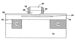
High performance integrated vertical transistors and method of making the same
PatentInactiveUS7217628B2
Innovation
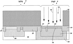
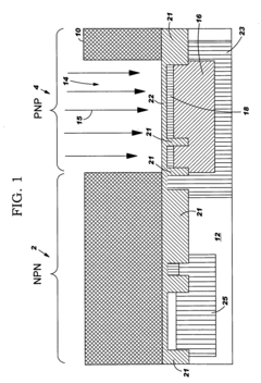
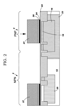
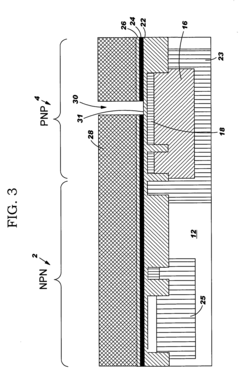
- The use of a shared silicon germanium (SiGe) low temperature epitaxial (LTE) layer allows for the fabrication of vertically aligned complementary bipolar transistors, where the epitaxially deposited extrinsic base of the NPN transistor serves as the emitter for the PNP transistor, and both transistors operate in a downward direction, utilizing advanced epitaxial techniques like molecular beam epitaxy (MBE) and low temperature epitaxy (LTE) to achieve identical vertical profiles.
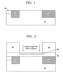
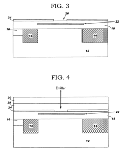
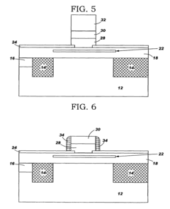
High performance vertical PNP transistor method
PatentInactiveUS20040248352A1
Innovation
- A method for fabricating high-performance vertical PNP transistors by incorporating an emitter region with silicon and germanium, sharing a single layer of silicon with the NPN transistor's base, and adding two additional masking steps to conventional CMOS and bipolar device fabrication processes, involving a SiGe low-temperature epitaxial layer and specific implantations to form the extrinsic and intrinsic bases.
Environmental Impact of PNP Transistor Manufacturing
The manufacturing process of PNP transistors, while essential for modern electronics, carries significant environmental implications. The production of these semiconductor devices involves complex processes that consume substantial energy and resources, potentially leading to various environmental impacts. One of the primary concerns is the high energy consumption during the manufacturing stages, particularly in the clean room environments required for semiconductor fabrication. These facilities demand constant climate control and air filtration, resulting in a considerable carbon footprint.
Material usage in PNP transistor production also raises environmental issues. The process requires rare and precious metals, such as gold and platinum, as well as potentially harmful chemicals like hydrofluoric acid and arsine gas. The extraction and processing of these materials can lead to habitat destruction, soil contamination, and water pollution in mining areas. Additionally, the use of toxic chemicals in the manufacturing process poses risks of environmental contamination if not properly managed and disposed of.
Water consumption is another critical environmental factor in PNP transistor production. The semiconductor industry is known for its high water usage, primarily for cleaning and cooling purposes. This extensive water consumption can strain local water resources, especially in water-scarce regions where many semiconductor facilities are located.
The disposal and recycling of electronic waste containing PNP transistors present further environmental challenges. As electronic devices become obsolete, improper disposal can lead to the leaching of harmful substances into soil and groundwater. The complex nature of these components makes recycling difficult, often resulting in e-waste being shipped to developing countries with less stringent environmental regulations.
Efforts to mitigate these environmental impacts are ongoing within the semiconductor industry. Many manufacturers are adopting more sustainable practices, such as implementing closed-loop water systems, increasing energy efficiency, and exploring alternative materials. Some companies are also investing in renewable energy sources to power their facilities and reduce their carbon footprint. Additionally, research into green chemistry alternatives for semiconductor production is progressing, aiming to replace hazardous substances with more environmentally friendly options.
The industry is also focusing on improving the recyclability and longevity of electronic components, including PNP transistors. This includes designing for easier disassembly and material recovery, as well as developing more durable components that extend the lifespan of electronic devices. Such initiatives not only reduce the environmental impact of manufacturing but also address the growing concern of electronic waste.
Scalability and Integration Challenges
As PNP transistor technology continues to advance, scalability and integration challenges have become increasingly prominent. The miniaturization of transistors has been a driving force in the semiconductor industry for decades, but as we approach the physical limits of silicon-based devices, new hurdles emerge in the realm of PNP transistor architectural design.
One of the primary challenges in scaling PNP transistors is maintaining performance while reducing size. As transistors shrink, issues such as short-channel effects and increased leakage currents become more pronounced. These effects can lead to reduced voltage gain, increased power consumption, and overall degradation of transistor performance. To address these challenges, researchers are exploring novel materials and structures, such as high-k dielectrics and metal gates, to improve electrostatic control and mitigate short-channel effects.
Integration challenges also arise as PNP transistors are incorporated into more complex circuits and systems. The need for higher levels of integration has led to the development of advanced packaging technologies, such as 3D integration and system-in-package (SiP) solutions. These approaches aim to maximize device density and minimize interconnect delays, but they also introduce new complexities in terms of thermal management and signal integrity.
Another significant challenge is the increasing variability in transistor characteristics as dimensions shrink. Process variations and random dopant fluctuations can lead to inconsistent performance across a chip, making it difficult to achieve uniform behavior in large-scale integrated circuits. This variability necessitates the development of more robust design methodologies and adaptive circuit techniques to ensure reliable operation.
The integration of PNP transistors with other semiconductor technologies, such as CMOS, presents additional challenges. Achieving compatibility between different process technologies while maintaining optimal performance for each device type requires careful consideration of fabrication processes and device architectures. This integration is crucial for creating more versatile and efficient mixed-signal circuits.
As the industry pushes towards more advanced nodes, the cost and complexity of manufacturing processes increase exponentially. The need for extreme ultraviolet (EUV) lithography and other sophisticated fabrication techniques adds significant challenges to the scalability of PNP transistor production. Balancing the trade-offs between performance, power consumption, and manufacturing costs becomes increasingly difficult as we approach the limits of traditional scaling.
To overcome these scalability and integration challenges, researchers are exploring alternative transistor architectures, such as vertical transistors and gate-all-around structures. These novel designs aim to provide better electrostatic control and improved scalability compared to traditional planar architectures. Additionally, the integration of new materials, such as III-V semiconductors and 2D materials, is being investigated to enhance carrier mobility and overcome the limitations of silicon.
Unlock deeper insights with Patsnap Eureka Quick Research — get a full tech report to explore trends and direct your research. Try now!
Generate Your Research Report Instantly with AI Agent
Supercharge your innovation with Patsnap Eureka AI Agent Platform!