How to Design Cost-Effective Circuits with PNP Transistors?
JUL 28, 20259 MIN READ
Generate Your Research Report Instantly with AI Agent
Patsnap Eureka helps you evaluate technical feasibility & market potential.
PNP Transistor Fundamentals and Design Goals
PNP transistors have been a fundamental component in electronic circuit design since their inception in the mid-20th century. These devices, characterized by their ability to control current flow using a small input signal, have played a crucial role in the development of modern electronics. The evolution of PNP transistor technology has been marked by continuous improvements in performance, efficiency, and cost-effectiveness.
The primary goal in designing cost-effective circuits with PNP transistors is to optimize their performance while minimizing overall production expenses. This involves a multifaceted approach that considers factors such as component selection, circuit topology, and manufacturing processes. Engineers aim to achieve a balance between functionality and cost, ensuring that the final product meets both technical specifications and economic constraints.
One of the key objectives in PNP transistor circuit design is to maximize the device's current gain, also known as beta (β). A higher current gain allows for more efficient amplification and switching operations, potentially reducing the number of components required in a circuit. This, in turn, can lead to lower production costs and improved reliability. Additionally, designers focus on minimizing power consumption, as energy-efficient circuits not only reduce operating costs but also extend battery life in portable devices.
Another critical aspect of cost-effective PNP transistor design is the optimization of thermal management. Efficient heat dissipation can allow for the use of smaller, less expensive heat sinks or even eliminate the need for additional cooling components altogether. This consideration becomes particularly important in high-power applications or densely packed circuit designs.
The miniaturization of PNP transistors and associated components is an ongoing trend that aligns with cost-effectiveness goals. Smaller transistors not only reduce material costs but also enable higher component density on printed circuit boards (PCBs). This leads to more compact designs, which can significantly lower manufacturing and packaging expenses.
In recent years, the integration of PNP transistors into more complex semiconductor devices, such as integrated circuits (ICs) and system-on-chip (SoC) solutions, has become increasingly common. This integration offers substantial cost benefits by reducing the number of discrete components, simplifying assembly processes, and improving overall system reliability.
As technology continues to advance, the design goals for PNP transistor circuits are expanding to include enhanced frequency response, improved noise characteristics, and better performance in extreme environmental conditions. These objectives drive innovation in materials science, fabrication techniques, and circuit design methodologies, all while maintaining a focus on cost-effectiveness.
Market Demand for PNP-based Circuits
The market demand for PNP-based circuits has been steadily growing, driven by the increasing need for cost-effective and efficient electronic solutions across various industries. PNP transistors, known for their ability to handle high currents and voltages, have found widespread applications in power management, amplification, and switching circuits.
In the consumer electronics sector, the demand for PNP-based circuits has surged due to the proliferation of portable devices and smart home appliances. These circuits play a crucial role in battery management systems, power supplies, and voltage regulators, contributing to improved energy efficiency and longer battery life in smartphones, tablets, and wearable devices.
The automotive industry has also emerged as a significant driver of demand for PNP-based circuits. With the rapid growth of electric and hybrid vehicles, there is an increased need for sophisticated power management and control systems. PNP transistors are essential components in motor drivers, battery management systems, and various sensor interfaces within modern vehicles.
Industrial automation and control systems represent another key market segment for PNP-based circuits. These circuits are widely used in programmable logic controllers (PLCs), motor drives, and sensor interfaces, enabling precise control and monitoring of industrial processes. The ongoing trend towards Industry 4.0 and smart manufacturing has further boosted the demand for reliable and cost-effective PNP-based solutions.
The telecommunications sector continues to be a significant consumer of PNP-based circuits, particularly in base station equipment and network infrastructure. These circuits are crucial for power amplification, signal processing, and voltage regulation in communication systems, supporting the expansion of 5G networks and the increasing data traffic.
In the medical device industry, PNP-based circuits find applications in various diagnostic and therapeutic equipment. From patient monitoring systems to portable medical devices, these circuits contribute to improved performance and reliability in critical healthcare applications.
The renewable energy sector has also witnessed growing demand for PNP-based circuits, particularly in solar inverters and wind turbine control systems. These circuits play a vital role in power conversion and management, enhancing the efficiency and reliability of renewable energy installations.
As the Internet of Things (IoT) continues to expand, the demand for low-power, cost-effective PNP-based circuits has increased significantly. These circuits are essential for sensor nodes, edge computing devices, and various IoT gateways, enabling efficient data collection and processing in smart city applications, environmental monitoring, and industrial IoT deployments.
Current Challenges in PNP Circuit Design
The design of cost-effective circuits using PNP transistors faces several significant challenges in the current technological landscape. One of the primary obstacles is the inherent limitations of PNP transistors compared to their NPN counterparts. PNP transistors typically have lower current gain, slower switching speeds, and higher parasitic capacitances, which can complicate circuit design and reduce overall performance.
Another major challenge lies in the power consumption of PNP-based circuits. As energy efficiency becomes increasingly critical in modern electronic devices, designers must find innovative ways to minimize power dissipation while maintaining circuit functionality. This often requires careful biasing and optimization of operating points, which can be more challenging with PNP transistors due to their characteristics.
The issue of temperature sensitivity also poses a significant hurdle in PNP circuit design. PNP transistors are generally more susceptible to temperature variations, which can lead to performance inconsistencies and reliability issues in diverse operating environments. Designers must implement robust temperature compensation techniques to ensure stable circuit operation across a wide range of conditions.
Cost-effectiveness in PNP circuit design is further complicated by the limited availability and higher cost of high-performance PNP transistors compared to NPN types. This scarcity often forces designers to make trade-offs between performance and cost, potentially compromising the overall circuit efficiency or functionality.
Integration challenges present another obstacle, particularly in mixed-signal and analog-digital interface circuits. The differing characteristics of PNP and NPN transistors can make it difficult to achieve balanced and symmetrical designs, especially in applications requiring precise matching or complementary operations.
Moreover, the increasing demand for miniaturization and higher integration density in electronic devices puts additional pressure on PNP circuit designers. Reducing component count while maintaining or improving performance becomes a complex balancing act, often requiring innovative circuit topologies and clever use of parasitic elements.
Lastly, the challenge of noise reduction in PNP circuits remains a persistent issue. PNP transistors typically exhibit higher noise levels compared to NPN transistors, which can be particularly problematic in low-signal applications or high-precision analog circuits. Designers must employ advanced noise reduction techniques and careful layout strategies to mitigate these effects and achieve the desired signal-to-noise ratio.
Cost-Effective PNP Circuit Solutions
01 Manufacturing processes for cost-effective PNP transistors
Various manufacturing techniques have been developed to produce cost-effective PNP transistors. These include optimized doping processes, improved lithography techniques, and innovative substrate materials. Such advancements help reduce production costs while maintaining or improving transistor performance.- Manufacturing process optimization: Improving the manufacturing process of PNP transistors can significantly reduce production costs. This includes optimizing epitaxial growth techniques, refining ion implantation processes, and developing more efficient doping methods. These advancements lead to higher yields, reduced material waste, and improved overall cost-effectiveness.
- Innovative device structures: Developing new PNP transistor structures can enhance performance while reducing manufacturing complexity and costs. This includes vertical and lateral PNP designs, as well as integrated structures that combine multiple components. These innovations can lead to smaller chip sizes, improved efficiency, and reduced production expenses.
- Material selection and optimization: Choosing and optimizing materials for PNP transistors can significantly impact cost-effectiveness. This includes exploring alternative substrate materials, optimizing dopant profiles, and developing new alloys for contacts and interconnects. Proper material selection can lead to improved performance, longer device lifetimes, and reduced production costs.
- Testing and quality control improvements: Enhancing testing and quality control processes can improve the overall cost-effectiveness of PNP transistor production. This includes developing more efficient testing methodologies, implementing automated inspection systems, and refining sorting and binning processes. These improvements can reduce defect rates, increase yield, and minimize post-production issues.
- Supply chain and production management: Optimizing supply chain and production management can significantly impact the cost-effectiveness of PNP transistors. This includes implementing just-in-time manufacturing, improving inventory management, and streamlining logistics. Effective management of these aspects can reduce overhead costs, minimize waste, and improve overall production efficiency.
02 Design optimization for cost-effective PNP transistors
Optimizing the design of PNP transistors can lead to improved cost-effectiveness. This includes reducing the size of transistors, optimizing the layout, and implementing innovative structures that enhance performance while minimizing material usage and production complexity.Expand Specific Solutions03 Integration of PNP transistors in cost-effective circuits
Integrating PNP transistors into larger circuits in a cost-effective manner involves careful design considerations. This includes optimizing circuit layouts, reducing component count, and implementing efficient power management strategies to maximize performance while minimizing overall costs.Expand Specific Solutions04 Cost-effective testing and quality control for PNP transistors
Implementing efficient testing and quality control processes is crucial for maintaining cost-effectiveness in PNP transistor production. This involves developing automated testing procedures, implementing statistical process control, and optimizing yield management techniques to reduce waste and improve overall production efficiency.Expand Specific Solutions05 Economic analysis and cost modeling for PNP transistor production
Conducting thorough economic analysis and cost modeling is essential for optimizing the cost-effectiveness of PNP transistor production. This includes evaluating material costs, production processes, and market demand to make informed decisions about manufacturing strategies and pricing.Expand Specific Solutions
Key Players in PNP Transistor Industry
The market for cost-effective PNP transistor circuit design is in a mature stage, with established players and well-developed technologies. The global semiconductor market size, which includes PNP transistors, is projected to reach $573 billion by 2022. Major companies like Infineon Technologies, STMicroelectronics, and Texas Instruments have high technological maturity in this field, offering advanced PNP transistor solutions. These industry leaders, along with emerging players such as GLOBALFOUNDRIES and Shanghai Huahong Grace Semiconductor, are driving innovation in miniaturization, power efficiency, and integration capabilities of PNP transistors, catering to diverse applications across automotive, consumer electronics, and industrial sectors.
Infineon Technologies AG
Technical Solution: Infineon has developed a cost-effective PNP transistor design using their proprietary OptiMOS technology. This approach integrates advanced trench gate structures with optimized doping profiles, resulting in reduced on-resistance and improved switching performance[1]. The company's PNP transistors feature a novel vertical structure that minimizes parasitic capacitances, enabling faster switching speeds and lower power dissipation[3]. Infineon has also implemented a unique emitter ballasting technique to enhance the device's safe operating area and reliability in high-current applications[5].
Strengths: Superior switching performance, reduced power losses, and enhanced reliability. Weaknesses: Potentially higher initial production costs and complexity in manufacturing processes.
International Business Machines Corp.
Technical Solution: IBM has developed a cost-effective PNP transistor design using their advanced SiGe BiCMOS technology. This approach incorporates a silicon-germanium base region, which significantly improves the transistor's current gain and frequency response[8]. IBM's PNP transistors feature a unique graded Ge profile in the base, which creates a built-in electric field that accelerates carrier transport[10]. The company has also implemented a self-aligned emitter-base structure that minimizes parasitic capacitances and resistances, resulting in improved switching performance[12].
Strengths: Excellent high-frequency performance, high current gain, and compatibility with CMOS integration. Weaknesses: Potentially higher manufacturing costs due to the use of SiGe materials.
Innovative PNP Circuit Topologies
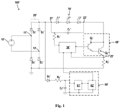
Driving circuit and associated lamp
PatentActiveUS20220232682A1
Innovation
- A driving circuit that directly charges an output capacitor from the mains supply in standby mode, maintaining a voltage lower than the LED's turn-on voltage but higher than a preset lowest voltage, allowing quick charging when switching to illumination mode, and utilizing a linear current source with zero or low voltage drop to reduce power consumption.
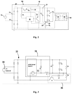
Integratable current source circuit
PatentInactiveEP0726512A3
Innovation
- A current source circuit design utilizing two npn transistors with specific resistor and diode configurations, along with an additional npn transistor, eliminates the need for pnp transistors, simplifying production and increasing the cut-off frequency with minimal additional circuitry, and can be expanded to a current mirror circuit with minimal components.
PNP vs NPN Cost-Benefit Analysis
When considering the design of cost-effective circuits, the choice between PNP and NPN transistors plays a crucial role in determining both performance and overall expenses. PNP transistors, while less common than their NPN counterparts, offer unique advantages in certain circuit configurations. However, their cost-benefit analysis reveals a complex interplay of factors that engineers must carefully consider.
From a cost perspective, PNP transistors are generally more expensive than NPN transistors due to their manufacturing process. The P-type semiconductor material used in PNP transistors is typically more challenging to produce, resulting in higher production costs. This price difference can be significant when designing circuits for large-scale production or cost-sensitive applications.
However, the cost analysis extends beyond the initial component price. PNP transistors can simplify circuit designs in specific scenarios, potentially reducing the overall number of components required. This simplification can lead to smaller PCB sizes, lower assembly costs, and improved reliability due to fewer potential points of failure. In applications where these factors are critical, the higher upfront cost of PNP transistors may be offset by long-term savings and performance benefits.
Performance-wise, PNP transistors exhibit different characteristics compared to NPN transistors. They typically have lower current gain and slower switching speeds, which can be a disadvantage in high-frequency applications. However, PNP transistors excel in certain circuit configurations, such as high-side switches and current sources, where their unique properties can be leveraged to create more efficient designs.
Energy efficiency is another crucial factor in the cost-benefit analysis. PNP transistors can be more energy-efficient in specific circuit topologies, particularly in low-power applications. This improved efficiency can translate to longer battery life in portable devices or reduced operating costs in industrial applications, providing long-term cost benefits that may outweigh the initial higher component cost.
Availability and supply chain considerations also factor into the cost-benefit equation. NPN transistors are more widely available and often have a broader range of specifications to choose from. This abundance can lead to more competitive pricing and easier sourcing. In contrast, the more limited selection of PNP transistors may result in supply chain challenges and potential cost increases due to scarcity.
When evaluating the cost-effectiveness of circuits using PNP transistors, designers must also consider the impact on manufacturing and testing processes. Some circuit designs using PNP transistors may require more complex assembly procedures or specialized testing equipment, potentially increasing production costs. However, these additional costs may be justified if the resulting circuit offers superior performance or reliability in the target application.
In conclusion, the cost-benefit analysis of PNP versus NPN transistors in circuit design is multifaceted. While PNP transistors are generally more expensive, their unique properties can lead to simplified designs, improved performance in specific applications, and potential long-term cost savings. Engineers must carefully weigh these factors against the initial component cost to determine the most cost-effective solution for their particular circuit requirements.
Environmental Impact of PNP Circuits
The environmental impact of PNP transistor circuits is an increasingly important consideration in the design and implementation of cost-effective electronic systems. As the demand for electronic devices continues to grow, so does the need for sustainable and environmentally friendly circuit designs. PNP transistors, while essential components in many electronic applications, can have both positive and negative effects on the environment throughout their lifecycle.
One of the primary environmental concerns associated with PNP circuits is the use of materials in their production. The manufacturing process of PNP transistors involves the use of various semiconductor materials, including silicon, germanium, and gallium arsenide. The extraction and processing of these materials can have significant environmental impacts, including habitat destruction, water pollution, and greenhouse gas emissions. Additionally, the production of PNP transistors often requires the use of toxic chemicals and solvents, which can pose risks to both human health and the environment if not properly managed.
However, the use of PNP transistors in circuit design can also contribute to positive environmental outcomes. By enabling more efficient and compact electronic devices, PNP circuits can help reduce overall energy consumption and material usage. This is particularly relevant in the context of portable electronics and IoT devices, where power efficiency is crucial. The improved performance and reduced power consumption of PNP-based circuits can lead to longer battery life and less frequent device replacements, ultimately reducing electronic waste.
The end-of-life phase of PNP circuits also presents environmental challenges and opportunities. Electronic waste containing PNP transistors can release harmful substances into the environment if not properly disposed of or recycled. However, advancements in recycling technologies are making it increasingly feasible to recover valuable materials from electronic components, including those found in PNP circuits. This not only reduces the environmental impact of electronic waste but also helps conserve natural resources by reducing the need for raw material extraction.
In recent years, there has been a growing focus on developing more environmentally friendly alternatives to traditional PNP transistors. Research into organic and biodegradable semiconductors shows promise for creating circuits with reduced environmental impact. These materials could potentially offer similar performance to conventional PNP transistors while being more easily recyclable and less harmful to the environment at the end of their lifecycle.
As the electronics industry continues to evolve, designers and manufacturers are increasingly considering the environmental impact of their products throughout the entire lifecycle. This holistic approach to circuit design, which takes into account the environmental implications of material selection, manufacturing processes, energy efficiency, and end-of-life management, is crucial for developing truly sustainable electronic systems. By carefully considering these factors in the design of cost-effective circuits with PNP transistors, it is possible to create innovative solutions that balance performance, affordability, and environmental responsibility.
Unlock deeper insights with Patsnap Eureka Quick Research — get a full tech report to explore trends and direct your research. Try now!
Generate Your Research Report Instantly with AI Agent
Supercharge your innovation with Patsnap Eureka AI Agent Platform!