How to Improve Signal Amplification Using PNP Transistors?
JUL 28, 202510 MIN READ
Generate Your Research Report Instantly with AI Agent
Patsnap Eureka helps you evaluate technical feasibility & market potential.
PNP Transistor Fundamentals and Objectives
PNP transistors have been a cornerstone of electronic circuit design since their inception in the mid-20th century. These semiconductor devices, characterized by their ability to control current flow, have played a crucial role in signal amplification across various applications. The fundamental principle of PNP transistors lies in their three-layer structure: a p-type emitter, an n-type base, and a p-type collector. This configuration allows for the control of current flow through the modulation of charge carriers, specifically holes, in the semiconductor material.
The evolution of PNP transistor technology has been marked by continuous improvements in manufacturing processes, materials, and design techniques. From the early germanium-based devices to modern silicon and compound semiconductor implementations, each iteration has brought enhanced performance characteristics. These advancements have consistently aimed at improving key parameters such as current gain, frequency response, and noise reduction, all of which are critical for effective signal amplification.
In the context of signal amplification, PNP transistors offer unique advantages over their NPN counterparts in certain circuit configurations. Their ability to source current from the emitter makes them particularly useful in applications where high-side current sensing or switching is required. Additionally, PNP transistors can provide complementary symmetry in push-pull amplifier stages, contributing to more efficient and balanced circuit designs.
The primary objective in improving signal amplification using PNP transistors revolves around optimizing several key aspects of transistor performance. These include enhancing the current gain (β or hFE), which directly impacts the amplification factor, and improving the frequency response to enable amplification of higher frequency signals. Furthermore, reducing noise contributions and minimizing distortion are crucial goals in achieving cleaner and more accurate signal amplification.
Another significant objective is to address the inherent limitations of PNP transistors, such as their typically lower switching speeds compared to NPN transistors. Overcoming these constraints through innovative circuit topologies and device engineering is essential for expanding the application range of PNP-based amplifiers. This includes exploring novel biasing techniques, feedback mechanisms, and multi-stage configurations that can leverage the strengths of PNP transistors while mitigating their weaknesses.
As we delve deeper into the realm of PNP transistor-based signal amplification, it becomes evident that the path forward involves a multifaceted approach. This encompasses not only improvements in device physics and fabrication but also advancements in circuit design methodologies and system-level optimizations. By focusing on these objectives, researchers and engineers aim to unlock new possibilities in signal processing, communication systems, and analog circuit design, pushing the boundaries of what can be achieved with PNP transistor technology.
Market Demand for Enhanced Signal Amplification
The demand for enhanced signal amplification using PNP transistors has been steadily growing across various industries, driven by the increasing need for high-performance electronic devices and systems. This market trend is particularly evident in sectors such as telecommunications, consumer electronics, automotive, and industrial automation.
In the telecommunications industry, the push for 5G and beyond technologies has created a significant demand for improved signal amplification solutions. PNP transistors play a crucial role in enhancing signal quality and range, which is essential for the deployment of next-generation wireless networks. The market for these components is expected to expand as telecom companies continue to upgrade their infrastructure.
Consumer electronics represent another major market segment driving the demand for enhanced signal amplification. With the proliferation of smart devices, including smartphones, tablets, and wearables, manufacturers are constantly seeking ways to improve signal processing capabilities while minimizing power consumption. PNP transistors offer a viable solution to this challenge, contributing to better audio quality, improved wireless connectivity, and extended battery life in portable devices.
The automotive industry is experiencing a rapid transformation towards electric and autonomous vehicles, creating new opportunities for signal amplification technologies. Advanced driver assistance systems (ADAS) and in-vehicle infotainment systems require robust signal processing capabilities to ensure reliable operation and enhanced user experience. PNP transistors are increasingly being utilized in these applications to improve signal integrity and reduce electromagnetic interference.
Industrial automation and control systems also contribute significantly to the market demand for enhanced signal amplification. As factories and manufacturing processes become more sophisticated and interconnected, the need for precise and reliable signal processing grows. PNP transistors are employed in various industrial applications, including sensor interfaces, motor control circuits, and data acquisition systems, where accurate signal amplification is critical for maintaining operational efficiency and product quality.
The medical device industry is another sector driving the demand for improved signal amplification technologies. Diagnostic equipment, patient monitoring systems, and implantable medical devices rely heavily on accurate signal processing to ensure reliable performance and patient safety. PNP transistors are utilized in these applications to amplify weak biological signals and improve the overall sensitivity of medical instruments.
As the Internet of Things (IoT) continues to expand, the demand for low-power, high-performance signal amplification solutions is expected to grow further. PNP transistors are well-suited for IoT applications due to their ability to operate efficiently at low voltages, making them ideal for battery-powered and energy-harvesting devices.
The market for enhanced signal amplification using PNP transistors is also influenced by the ongoing miniaturization trend in electronics. As devices become smaller and more compact, the need for efficient signal amplification in limited spaces becomes increasingly important. PNP transistors offer a compact solution that can be easily integrated into densely packed circuit designs.
Current Challenges in PNP Transistor Amplification
Despite the widespread use of PNP transistors in signal amplification, several challenges persist in maximizing their performance and efficiency. One of the primary issues is the inherent lower mobility of holes compared to electrons, which results in reduced current gain and slower switching speeds in PNP transistors. This limitation becomes particularly pronounced in high-frequency applications, where PNP transistors often struggle to match the performance of their NPN counterparts.
Another significant challenge lies in the base-width modulation effect, also known as the Early effect. This phenomenon causes the effective base width to vary with collector-emitter voltage, leading to undesirable changes in current gain and output resistance. As a result, achieving stable and consistent amplification across different operating conditions becomes more difficult with PNP transistors.
Temperature sensitivity presents yet another hurdle in PNP transistor amplification. The current gain of PNP transistors tends to be more temperature-dependent than that of NPN transistors, which can lead to performance variations and potential instability in amplifier circuits. This sensitivity necessitates careful thermal management and compensation techniques to maintain consistent amplification characteristics.
The presence of parasitic capacitances, particularly the collector-base capacitance, poses challenges in high-frequency applications. These capacitances limit the transistor's ability to respond quickly to input signals, resulting in reduced bandwidth and potential signal distortion. Minimizing the impact of these parasitic elements while maintaining other performance parameters remains a complex balancing act.
Power handling capabilities of PNP transistors also present limitations in certain amplification scenarios. Generally, PNP transistors have lower power handling capacities compared to their NPN counterparts, which can restrict their use in high-power amplification applications. This constraint often necessitates the use of multiple devices or alternative circuit topologies to achieve the desired output power levels.
Noise performance is another area where PNP transistors face challenges. The inherent characteristics of PNP devices can lead to higher noise figures compared to NPN transistors, particularly at higher frequencies. This increased noise can degrade the signal-to-noise ratio in sensitive amplification applications, requiring additional noise reduction techniques or alternative device selection.
Lastly, the manufacturing process for high-performance PNP transistors tends to be more complex and costly than that of NPN transistors. This complexity can result in higher device costs and potential limitations in availability, particularly for specialized or high-performance applications. Balancing performance requirements with cost considerations remains an ongoing challenge in PNP transistor amplification design.
Existing PNP Amplification Techniques
01 PNP transistor structure and fabrication
This category focuses on the design and manufacturing processes of PNP transistors. It includes innovations in the structure of PNP transistors, such as improvements in the emitter, base, and collector regions, as well as novel fabrication techniques to enhance performance and reduce size.- PNP transistor structure and fabrication: This category focuses on the design and manufacturing processes of PNP transistors. It includes innovations in the structure of PNP transistors, such as improvements in the emitter, base, and collector regions, as well as novel fabrication techniques to enhance performance and reduce size. These advancements contribute to better signal amplification capabilities.
- Signal amplification circuits using PNP transistors: This category covers various circuit designs that utilize PNP transistors for signal amplification. It includes different configurations and topologies that optimize the use of PNP transistors to achieve higher gain, improved linearity, and better frequency response in amplification circuits.
- Complementary bipolar transistor circuits: This category focuses on circuits that combine PNP and NPN transistors to achieve improved performance in signal amplification. These complementary designs often result in better power efficiency, reduced distortion, and enhanced temperature stability compared to circuits using only one type of transistor.
- High-frequency applications of PNP transistors: This category covers the use of PNP transistors in high-frequency signal amplification applications. It includes techniques to improve the frequency response of PNP transistors, such as reducing parasitic capacitances and optimizing the transistor geometry for high-speed operation.
- Integration of PNP transistors in semiconductor devices: This category focuses on the integration of PNP transistors with other semiconductor components to create more complex and efficient signal amplification systems. It includes innovations in combining PNP transistors with other devices on a single chip, as well as techniques to improve overall system performance and reduce power consumption.
02 Signal amplification circuits using PNP transistors
This point covers various circuit designs that utilize PNP transistors for signal amplification. It includes different configurations and topologies that leverage the characteristics of PNP transistors to achieve improved gain, bandwidth, and noise performance in amplifier circuits.Expand Specific Solutions03 PNP transistors in integrated circuits
This category deals with the integration of PNP transistors into larger integrated circuit designs. It includes techniques for incorporating PNP transistors alongside other components, such as NPN transistors and passive elements, to create complex analog and mixed-signal circuits on a single chip.Expand Specific Solutions04 Biasing and temperature compensation for PNP transistors
This point focuses on methods and circuits for properly biasing PNP transistors and compensating for temperature-induced variations in their performance. It includes techniques for maintaining stable operating points and ensuring consistent amplification across different environmental conditions.Expand Specific Solutions05 High-frequency applications of PNP transistors
This category covers the use of PNP transistors in high-frequency signal amplification and processing. It includes design considerations and circuit topologies that optimize PNP transistor performance for applications such as RF amplifiers, oscillators, and mixers in communication systems.Expand Specific Solutions
Key Players in Semiconductor Industry
The signal amplification using PNP transistors market is in a mature stage, with established players and well-understood technology. The global market size for transistors, including PNP types, is estimated to be in the billions of dollars. Technologically, PNP transistors are well-developed, with ongoing incremental improvements in performance and efficiency. Key players in this field include International Business Machines Corp., Infineon Technologies AG, and QUALCOMM, Inc., who are continually innovating to enhance signal amplification techniques. These companies, along with others like Texas Instruments and Renesas Electronics Corp., are investing in research and development to push the boundaries of PNP transistor capabilities, focusing on areas such as power efficiency, miniaturization, and integration with other semiconductor technologies.
Infineon Technologies AG
Technical Solution: Infineon has made significant strides in PNP transistor technology for signal amplification, particularly in their automotive and industrial product lines. They have developed a proprietary SiGe:C (Silicon-Germanium-Carbon) process that enables the creation of high-speed PNP transistors with improved current gain and cutoff frequency[4]. Infineon's approach includes the use of advanced epitaxial growth techniques to create precise doping profiles and reduce base transit time. Their PNP transistors feature optimized emitter geometry and reduced parasitic capacitances, resulting in enhanced high-frequency performance and improved linearity[5]. Infineon has also focused on integrating these advanced PNP transistors into their power management ICs and audio amplifier products, offering improved efficiency and signal quality[6].
Strengths: High-speed PNP transistors with excellent high-frequency performance. Well-suited for automotive and industrial applications. Weaknesses: May have higher production costs due to advanced manufacturing processes. Potentially limited availability compared to more common transistor types.
QUALCOMM, Inc.
Technical Solution: Qualcomm has made significant advancements in PNP transistor technology for signal amplification, particularly in the context of mobile and wireless communication systems. Their approach focuses on integrating high-performance PNP transistors into their RF front-end modules and power management ICs. Qualcomm has developed a proprietary BiCMOS process that allows for the creation of PNP transistors with improved current gain and frequency response[7]. They have implemented advanced techniques such as selective epitaxial growth and self-aligned emitter-base structures to reduce parasitic capacitances and improve overall transistor performance. Qualcomm's PNP transistors feature optimized doping profiles and reduced base width, resulting in enhanced high-frequency characteristics and lower noise figures[8]. These improvements have been crucial in developing more efficient and compact RF amplifiers for 5G and other wireless technologies[9].
Strengths: High-performance PNP transistors optimized for RF and mobile applications. Excellent integration with other wireless technologies. Weaknesses: Primarily focused on mobile and wireless applications, potentially limiting use in other sectors. May require specialized design considerations for implementation.
Innovative PNP Circuit Designs
Apparatus using PNP bipolar transistor as buffer to drive video signal
PatentInactiveUS6468201B1
Innovation
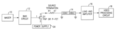
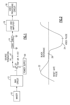
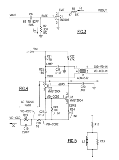
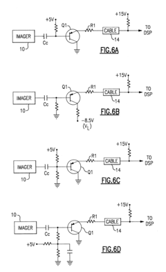
- A PNP bipolar transistor or enhancement mode P-channel FET is used as a buffer at the distal end of the endoscope, biased by a base bias circuit and power supply located near the transistor, with the emitter connected through a cable to a load at the proximal end, to drive video signals from the imager to video processing circuits, employing a bias circuit and power supply to maintain signal integrity and reduce power dissipation.
Nucleic acid amplification methods
PatentWO2021231263A2
Innovation
- A method involving strand-displacing polymerases to amplify polynucleotides with continuous strands, using a combination of forward and reverse primers on solid supports, allowing for multiple cycles of denaturation, hybridization, and extension to generate longer amplicons, enhancing amplification efficiency and cluster brightness.
Noise Reduction Strategies in PNP Circuits
Noise reduction is a critical aspect of signal amplification in PNP transistor circuits. Effective strategies for minimizing noise can significantly enhance the overall performance and reliability of these circuits. One primary approach involves implementing proper shielding techniques. This includes using conductive enclosures to protect sensitive components from electromagnetic interference (EMI) and radio frequency interference (RFI). Additionally, careful PCB layout design can help reduce noise by minimizing signal path lengths and separating analog and digital grounds.
Another key strategy is the use of decoupling capacitors. These components help to filter out high-frequency noise from power supply lines, ensuring a cleaner voltage supply to the PNP transistors. Placing decoupling capacitors close to the transistors and other active components can effectively reduce noise coupling through power rails.
Implementing differential signaling techniques can also contribute to noise reduction in PNP circuits. By using balanced transmission lines and differential amplifiers, common-mode noise can be effectively cancelled out, resulting in a cleaner signal. This approach is particularly useful in environments with high electromagnetic interference.
Proper biasing of PNP transistors is crucial for noise reduction. Ensuring that the transistors operate in their optimal region can minimize noise generation within the device itself. This involves careful selection of resistor values in the biasing network to achieve the desired operating point while maintaining low noise characteristics.
Utilizing low-noise components is another effective strategy. Selecting PNP transistors with low noise figures and high-quality passive components can significantly reduce the overall noise in the circuit. Special attention should be paid to the selection of resistors, as they can be a significant source of thermal noise.
Implementing feedback mechanisms, such as negative feedback loops, can help reduce noise by stabilizing the circuit's operation and minimizing distortion. This technique can be particularly effective in amplifier stages using PNP transistors.
Filtering techniques play a crucial role in noise reduction. Incorporating well-designed low-pass, high-pass, or band-pass filters at strategic points in the circuit can effectively remove unwanted frequency components, thereby reducing noise. The choice of filter type and cutoff frequencies should be carefully considered based on the specific application requirements.
Lastly, temperature management is an often-overlooked aspect of noise reduction in PNP circuits. Maintaining a stable operating temperature through proper heat sinking and thermal design can help minimize temperature-dependent noise sources, such as thermal noise in resistors and shot noise in transistors.
Thermal Management in PNP Amplifiers
Thermal management is a critical aspect of PNP transistor amplifier design, directly impacting performance, reliability, and efficiency. As PNP transistors amplify signals, they generate heat due to power dissipation, which can lead to thermal runaway and device failure if not properly managed. Effective thermal management strategies are essential to maintain optimal operating temperatures and ensure stable amplifier performance.
One of the primary thermal management techniques for PNP amplifiers is the use of heat sinks. These passive cooling devices increase the surface area available for heat dissipation, allowing for more efficient transfer of thermal energy from the transistor to the surrounding environment. The selection of an appropriate heat sink depends on factors such as the power dissipation of the transistor, ambient temperature, and available space within the amplifier design.
Active cooling methods, such as forced-air cooling or liquid cooling systems, can be employed in high-power applications where passive cooling alone is insufficient. Forced-air cooling utilizes fans or blowers to increase air circulation around the transistor and heat sink, enhancing convective heat transfer. Liquid cooling systems, while more complex and costly, offer superior thermal management capabilities for extremely high-power applications.
Thermal interface materials (TIMs) play a crucial role in improving heat transfer between the transistor and heat sink. These materials, such as thermal greases, pads, or adhesives, fill microscopic air gaps at the interface, reducing thermal resistance and improving overall heat dissipation efficiency. The selection of an appropriate TIM depends on factors such as thermal conductivity, ease of application, and long-term reliability.
Circuit board design also plays a significant role in thermal management. Proper component placement and PCB layout can help distribute heat more evenly across the board, preventing localized hot spots. The use of thermal vias, which are plated through-holes that conduct heat from one PCB layer to another, can further enhance heat dissipation by creating additional thermal pathways.
Temperature monitoring and control systems are often implemented to ensure safe and reliable operation of PNP amplifiers. These systems may include temperature sensors, thermal shutdown circuits, and feedback mechanisms to adjust operating parameters based on temperature readings. Such active thermal management approaches can prevent thermal runaway and extend the lifespan of the amplifier.
Advancements in semiconductor materials and packaging technologies have also contributed to improved thermal management in PNP amplifiers. For example, the development of high-temperature semiconductor materials and advanced packaging techniques has led to transistors with better thermal performance and higher maximum operating temperatures.
In conclusion, effective thermal management in PNP amplifiers requires a multifaceted approach, combining passive and active cooling techniques, careful circuit design, and advanced materials. By implementing these strategies, designers can optimize signal amplification performance while ensuring long-term reliability and efficiency of PNP transistor-based amplifiers.
Unlock deeper insights with Patsnap Eureka Quick Research — get a full tech report to explore trends and direct your research. Try now!
Generate Your Research Report Instantly with AI Agent
Supercharge your innovation with Patsnap Eureka AI Agent Platform!