

How to Scale Down PNP Transistor Size Without Compromising Efficiency?
JUL 28, 20259 MIN READ
Generate Your Research Report Instantly with AI Agent
PatSnap Eureka helps you evaluate technical feasibility & market potential.
PNP Transistor Scaling Background and Objectives
PNP transistors have been a cornerstone of semiconductor technology since their inception in the mid-20th century. As the demand for smaller, more efficient electronic devices continues to grow, the need to scale down PNP transistor size while maintaining or improving efficiency has become a critical challenge in the semiconductor industry.
The evolution of PNP transistor technology has been closely tied to the overall progress in semiconductor manufacturing. From the early germanium-based devices to modern silicon and compound semiconductor implementations, PNP transistors have undergone significant improvements in size, performance, and reliability. However, as we approach the physical limits of traditional scaling techniques, new approaches are required to continue this trend.
The primary objective of scaling down PNP transistor size is to increase the density of transistors on a chip, thereby improving overall performance and reducing power consumption. This goal aligns with the broader industry trend of miniaturization and increased functionality in electronic devices. However, as transistors shrink, various challenges emerge, including increased leakage current, reduced carrier mobility, and degraded thermal characteristics.
Efficiency in PNP transistors is typically measured by factors such as current gain, switching speed, and power dissipation. Maintaining or improving these parameters while reducing size is a complex task that requires innovations in materials science, device physics, and fabrication techniques. The industry has set ambitious targets for transistor scaling, with some roadmaps aiming for sub-5nm node technologies in the near future.
Recent technological advancements have opened up new possibilities for PNP transistor scaling. These include the development of novel materials like silicon-germanium alloys, the implementation of strain engineering techniques, and the exploration of vertical transistor architectures. Additionally, emerging technologies such as tunnel field-effect transistors (TFETs) and negative capacitance FETs offer potential alternatives to traditional PNP designs for certain applications.
The quest for smaller, more efficient PNP transistors is driven not only by the need for improved performance but also by economic factors. As the cost of semiconductor manufacturing continues to rise, achieving higher transistor densities becomes crucial for maintaining the economic viability of chip production. This economic pressure further underscores the importance of finding innovative solutions to the scaling challenge.
In conclusion, the background of PNP transistor scaling reflects a history of continuous innovation and the relentless pursuit of improved performance. The objectives for future scaling efforts are clear: to push the boundaries of size reduction while enhancing efficiency, thereby enabling the next generation of advanced electronic devices and systems. This goal presents both significant challenges and exciting opportunities for researchers and engineers in the semiconductor industry.
Market Demand for Miniaturized PNP Transistors
The market demand for miniaturized PNP transistors has been steadily increasing, driven by the relentless pursuit of smaller, more efficient electronic devices across various industries. As consumer electronics continue to shrink in size while expanding in functionality, the need for compact transistors that maintain high performance has become paramount.
In the smartphone industry, manufacturers are constantly striving to reduce device thickness and weight while increasing battery life and processing power. This has led to a surge in demand for smaller PNP transistors that can operate efficiently within tighter spaces. The wearable technology sector, including smartwatches and fitness trackers, also requires ultra-compact components to achieve sleek designs and extended battery life.
The automotive industry is another significant driver of demand for miniaturized PNP transistors. As vehicles become more electrified and incorporate advanced driver assistance systems (ADAS), the need for compact, high-performance transistors has grown exponentially. These components are essential for power management, sensor systems, and various control units throughout modern vehicles.
In the industrial sector, the trend towards miniaturization is evident in the development of smaller, more efficient robotics and automation systems. Compact PNP transistors play a crucial role in these applications, enabling precise control and power management in confined spaces. The Internet of Things (IoT) ecosystem has further fueled the demand for miniaturized transistors, as connected devices become more prevalent in both consumer and industrial settings.
The medical device industry has also contributed to the growing market for miniaturized PNP transistors. Implantable medical devices, portable diagnostic equipment, and wearable health monitors all benefit from smaller, more efficient components that can operate reliably within the human body or in close proximity to it.
As 5G technology continues to roll out globally, the telecommunications infrastructure sector has seen an increased need for compact, high-performance transistors. Base stations and small cell deployments require miniaturized components to achieve the desired network density and performance while minimizing physical footprint.
The aerospace and defense industries have likewise shown a strong interest in miniaturized PNP transistors. Satellites, drones, and advanced avionics systems all benefit from reduced size and weight, making compact transistors essential for these applications.
Overall, the market demand for miniaturized PNP transistors is expected to continue its upward trajectory as industries across the board prioritize smaller form factors, improved energy efficiency, and enhanced performance in their electronic systems and devices.
Current Challenges in PNP Transistor Scaling
The scaling down of PNP transistors presents several significant challenges that researchers and engineers must overcome to maintain or improve device efficiency. One of the primary obstacles is the increased impact of short-channel effects as transistor dimensions shrink. These effects, including drain-induced barrier lowering (DIBL) and threshold voltage roll-off, become more pronounced at smaller scales, leading to increased leakage currents and reduced control over the device's electrical characteristics.
Another critical challenge is the management of parasitic capacitances and resistances. As transistor size decreases, the relative impact of these parasitic elements grows, potentially degrading switching speed and power efficiency. The reduction in channel length also leads to velocity saturation of charge carriers, limiting the expected performance gains from scaling.
The issue of quantum mechanical effects becomes increasingly significant as dimensions approach the nanometer scale. Phenomena such as quantum tunneling through the gate oxide and between source and drain regions can lead to increased off-state current and reduced on/off current ratios, compromising the transistor's switching capabilities.
Heat dissipation presents another major hurdle in PNP transistor scaling. Smaller devices generate higher power densities, making it more difficult to efficiently remove heat from the active regions. This can lead to thermal runaway and reliability issues if not properly addressed.
Dopant fluctuations and random dopant placement become more problematic at smaller scales. The statistical variations in dopant distribution can lead to significant device-to-device variability, affecting threshold voltage and other critical parameters. This variability can impact circuit performance and yield in large-scale integrated systems.
Manufacturing challenges also increase with scaling. Achieving precise control over critical dimensions, such as gate length and oxide thickness, becomes more difficult as sizes decrease. Advanced lithography techniques and new materials are often required to overcome these limitations, adding complexity and cost to the fabrication process.
The need for ultra-thin gate dielectrics to maintain electrostatic control over the channel presents its own set of challenges. As oxide thickness decreases, gate leakage due to direct tunneling increases exponentially, necessitating the exploration of high-k dielectric materials and metal gates to mitigate this issue.
Addressing these challenges requires a multifaceted approach, combining innovations in device architecture, materials science, and fabrication techniques. Researchers are exploring various strategies, including strain engineering, novel channel materials, and three-dimensional transistor structures, to overcome the limitations imposed by traditional scaling methods and continue improving PNP transistor performance at smaller dimensions.
Existing PNP Transistor Scaling Techniques
01 Transistor size reduction techniques
Various methods are employed to reduce the size of PNP transistors, including advanced lithography techniques, improved doping processes, and novel device structures. These techniques aim to minimize the physical dimensions of the transistor while maintaining or enhancing its performance characteristics.- Transistor size reduction techniques: Various methods are employed to reduce the size of PNP transistors, including advanced lithography techniques, vertical integration, and optimized doping profiles. These techniques allow for the creation of smaller, more efficient transistors while maintaining or improving performance characteristics.
- Emitter-base junction optimization: Optimizing the emitter-base junction is crucial for PNP transistor size reduction. This involves careful control of doping concentrations, junction depths, and lateral diffusion to minimize parasitic capacitances and improve switching speeds while maintaining a compact device structure.
- Integration with other semiconductor devices: PNP transistors are often integrated with other semiconductor devices such as NPN transistors, resistors, and capacitors to form complex circuits. The size of PNP transistors must be optimized in relation to these other components to achieve overall circuit miniaturization and improved performance.
- High-frequency performance optimization: Reducing the size of PNP transistors while maintaining or improving high-frequency performance is a key challenge. This involves careful design of the transistor structure, including base width reduction, collector resistance minimization, and parasitic capacitance reduction.
- Packaging and thermal management: As PNP transistor sizes decrease, packaging and thermal management become increasingly important. Advanced packaging techniques and materials are used to ensure proper heat dissipation and electrical connectivity while maintaining a small overall device footprint.
02 Vertical PNP transistor structures
Vertical PNP transistor designs are utilized to optimize device performance and reduce overall size. These structures feature vertically aligned p-n junctions, allowing for more efficient current flow and improved high-frequency operation while minimizing the transistor's footprint.Expand Specific Solutions03 Integration of PNP transistors in ICs
PNP transistors are integrated into various integrated circuit (IC) designs, with a focus on optimizing size and performance. This integration involves careful consideration of layout techniques, interconnect strategies, and process compatibility to achieve compact and efficient circuit designs.Expand Specific Solutions04 Scaling of PNP transistor parameters
The scaling of PNP transistor parameters, such as base width, emitter area, and collector-base capacitance, is crucial for size reduction. This scaling process involves careful optimization of device geometry and doping profiles to maintain desired electrical characteristics while minimizing physical dimensions.Expand Specific Solutions05 Novel materials for PNP transistor fabrication
The use of novel materials in PNP transistor fabrication enables further size reduction and performance enhancement. These materials may include advanced semiconductors, insulators, or metal alloys that offer improved electrical properties or allow for more precise control of device dimensions during manufacturing.Expand Specific Solutions
Key Players in PNP Transistor Manufacturing
The competition in scaling down PNP transistor size while maintaining efficiency is at a mature stage, with significant market potential and ongoing technological advancements. The global semiconductor industry, valued at over $500 billion, sees major players like TSMC, Intel, and Qualcomm investing heavily in this area. These companies, along with others like IBM and Samsung, are pushing the boundaries of transistor miniaturization, reaching sub-10nm nodes. The technology's maturity is evident in the widespread adoption of advanced manufacturing processes by key players, with TSMC and Intel leading in 5nm and 7nm technologies. However, challenges in maintaining efficiency at smaller scales continue to drive innovation and competition among industry leaders.
TAIWAN SEMICONDUCTOR CO., LTD.
Technical Solution: TSMC has developed advanced FinFET technology to scale down PNP transistor size while maintaining efficiency. Their N3 (3nm) process node utilizes Gate-All-Around (GAA) nanosheet transistors, which offer better electrostatic control and reduced short-channel effects compared to traditional FinFETs[1]. This allows for further miniaturization of PNP transistors without compromising performance. TSMC's approach includes optimizing channel materials, reducing parasitic capacitance, and implementing strain engineering techniques to enhance carrier mobility[2]. They have also introduced high-mobility channel materials like SiGe for PMOS devices, which can improve hole mobility and overall transistor efficiency[3].
Strengths: Industry-leading process technology, high volume manufacturing capability, and extensive R&D resources. Weaknesses: High capital expenditure requirements and potential geopolitical risks.
Intel Corp.
Technical Solution: Intel's approach to scaling down PNP transistor size focuses on their RibbonFET technology, which is their implementation of GAA transistors. This design allows for increased current flow and improved electrical signals while reducing the transistor footprint[4]. Intel's 20A process node incorporates PowerVia, a backside power delivery method that reduces resistance and improves power efficiency in smaller transistors[5]. They have also developed strained silicon techniques and high-k metal gates to enhance carrier mobility and reduce leakage current in scaled-down devices. Intel's SuperFin technology, introduced in their 10nm process, uses novel high-performance metal stacks and enhanced epitaxial growth of crystal structures to improve transistor performance at smaller sizes[6].
Strengths: Vertical integration of design and manufacturing, strong research capabilities. Weaknesses: Historical delays in process node advancements, catching up to competitors in leading-edge nodes.
Innovative Approaches to PNP Transistor Scaling
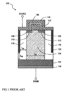
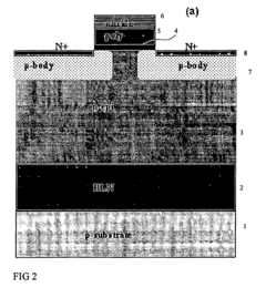
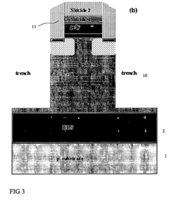
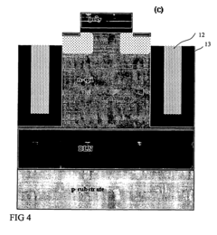
Method of making a transistor
PatentActiveEP1717865B1
Innovation
- A self-aligned method of manufacturing transistors is introduced, where a control electrode structure is formed first, followed by the creation of spacers and trenches, allowing for reduced dimensions and improved alignment, which reduces on-resistance by enabling higher doping concentrations in the drift region without precise doping matching, and allows for more integrated transistor cells per unit area.
CMOS device and fabricating method thereof
PatentActiveUS7615434B2
Innovation
- A fabricating method for CMOS devices involves forming stress layers with a liner layer as a hard mask to avoid direct damage during photoresist removal, using silicon oxide, silicon oxynitride, or amorphous carbon as the liner layer and silicon nitride as the stress layer, allowing for the creation of tensile and compressive stress on both N-type and P-type MOS transistors.
Material Advancements for PNP Transistor Scaling
Material advancements play a crucial role in scaling down PNP transistor size while maintaining or improving efficiency. Recent developments in semiconductor materials have opened up new possibilities for miniaturization and performance enhancement. Silicon-germanium (SiGe) alloys have emerged as a promising material for PNP transistors, offering improved carrier mobility and reduced parasitic capacitance compared to traditional silicon-based devices.
The incorporation of high-k dielectric materials, such as hafnium oxide (HfO2) and zirconium oxide (ZrO2), has enabled further scaling of transistor dimensions. These materials allow for thinner gate dielectrics without compromising the gate capacitance, leading to better electrostatic control and reduced leakage currents. Additionally, the use of metal gates in conjunction with high-k dielectrics has helped mitigate issues related to gate depletion and boron penetration in PNP transistors.
Advanced strain engineering techniques have been developed to enhance carrier mobility in PNP transistors. Compressive strain applied to the channel region can significantly improve hole mobility, leading to higher drive currents and faster switching speeds. This can be achieved through various methods, including the use of silicon-germanium source/drain regions or the application of stress liners.
The introduction of novel channel materials, such as germanium and III-V compounds, has shown promise for future PNP transistor scaling. These materials offer superior hole mobility compared to silicon, potentially enabling higher performance at smaller dimensions. However, challenges related to integration with existing silicon-based processes and manufacturing infrastructure need to be addressed for widespread adoption.
Advancements in doping techniques have also contributed to PNP transistor scaling. Ultra-shallow junction formation through techniques like low-energy ion implantation and advanced annealing processes has allowed for better control of dopant profiles and reduced short-channel effects. Additionally, the development of in-situ doped epitaxial growth processes has enabled the creation of highly controlled and abrupt doping profiles.
The exploration of two-dimensional (2D) materials, such as transition metal dichalcogenides (TMDs), has opened up new avenues for extreme transistor scaling. These atomically thin materials offer unique electronic properties and the potential for ultimate vertical scaling. While still in the research phase, 2D materials could potentially revolutionize PNP transistor design and scaling in the future.
Environmental Impact of PNP Transistor Production
The environmental impact of PNP transistor production is a critical consideration as the semiconductor industry strives to scale down transistor sizes while maintaining efficiency. The manufacturing process of PNP transistors involves several stages that can have significant environmental implications, particularly as production scales up to meet increasing demand for smaller, more efficient devices.
One of the primary environmental concerns is the use of hazardous materials in the fabrication process. The production of PNP transistors requires various chemicals, including dopants, etchants, and cleaning agents, many of which are toxic and potentially harmful to the environment if not properly managed. As transistor sizes decrease, the precision required in manufacturing increases, often leading to more intensive use of these chemicals and potentially greater environmental risks.
Water consumption is another major environmental factor in PNP transistor production. The semiconductor manufacturing process is water-intensive, with large volumes used for cleaning and cooling. As transistors become smaller, the need for ultra-pure water increases, putting additional strain on local water resources. This is particularly concerning in regions where water scarcity is already an issue.
Energy consumption in the production of PNP transistors is substantial, contributing to the industry's carbon footprint. The high-precision equipment required for manufacturing smaller transistors often demands more energy to operate. Clean room environments, essential for producing miniaturized components, are also energy-intensive due to the need for constant air filtration and temperature control.
Waste management is a crucial aspect of the environmental impact of PNP transistor production. The manufacturing process generates various types of waste, including chemical byproducts, contaminated water, and discarded materials. As transistor sizes decrease, the complexity of waste management increases, requiring more sophisticated treatment and disposal methods to minimize environmental harm.
The sourcing of raw materials for PNP transistor production also has environmental implications. The extraction and processing of semiconductor materials can lead to habitat destruction, soil erosion, and water pollution. As demand for these materials grows with the push for smaller transistors, the environmental impact of mining and refining activities may intensify.
Efforts to mitigate the environmental impact of PNP transistor production are ongoing. Many semiconductor manufacturers are implementing more sustainable practices, such as recycling water and chemicals, improving energy efficiency, and exploring alternative materials. However, as the industry continues to pursue smaller transistor sizes, balancing technological advancement with environmental responsibility remains a significant challenge.
In conclusion, while scaling down PNP transistor size offers potential benefits in terms of device efficiency and performance, it also presents complex environmental challenges. The semiconductor industry must continue to innovate not only in transistor technology but also in sustainable manufacturing practices to minimize the ecological footprint of PNP transistor production.
Unlock deeper insights with PatSnap Eureka Quick Research — get a full tech report to explore trends and direct your research. Try now!
Generate Your Research Report Instantly with AI Agent
Supercharge your innovation with PatSnap Eureka AI Agent Platform!