

PNP Transistor Integration in IoT Devices: Current Developments
JUL 28, 20259 MIN READ
Generate Your Research Report Instantly with AI Agent
PatSnap Eureka helps you evaluate technical feasibility & market potential.
PNP Transistor Evolution and IoT Integration Goals
PNP transistors have played a crucial role in the evolution of electronic devices since their inception in the mid-20th century. Initially developed as a complement to NPN transistors, PNP transistors have undergone significant advancements in terms of size, efficiency, and functionality. The journey of PNP transistors from large, discrete components to integrated circuit elements has been marked by continuous improvements in manufacturing processes and materials science.
In the context of IoT devices, the integration of PNP transistors represents a critical technological advancement. The primary goal of this integration is to enhance the performance, energy efficiency, and functionality of IoT devices while minimizing their size and cost. PNP transistors offer unique advantages in low-power applications, making them particularly suitable for battery-operated IoT devices that require long operational lifetimes.
The evolution of PNP transistors in IoT devices has been driven by several key objectives. Firstly, there is a strong focus on reducing power consumption to extend battery life in wireless sensors and wearable devices. This has led to the development of ultra-low-power PNP transistors capable of operating at sub-threshold voltages. Secondly, miniaturization efforts have resulted in the creation of nanoscale PNP transistors, enabling higher integration densities and more compact IoT devices.
Another significant goal in PNP transistor integration for IoT is improving their high-frequency performance. This is crucial for applications requiring fast data processing and communication, such as in smart home devices and industrial IoT sensors. Researchers and manufacturers are exploring novel materials and structures to enhance the switching speed and frequency response of PNP transistors without compromising their low-power characteristics.
The integration of PNP transistors in IoT devices also aims to address specific challenges posed by the IoT environment. These include enhancing resistance to electromagnetic interference, improving thermal management, and increasing reliability under varying environmental conditions. As IoT devices are often deployed in harsh or remote locations, the durability and longevity of PNP transistors become paramount considerations in their design and integration.
Looking ahead, the future goals for PNP transistor integration in IoT devices include further advancements in energy harvesting capabilities, enabling self-powered IoT nodes. Additionally, there is a growing interest in developing PNP transistors that can operate efficiently across a wider temperature range, expanding the potential applications of IoT devices in extreme environments.
IoT Market Demand for PNP Transistors
The Internet of Things (IoT) market has shown a significant and growing demand for PNP transistors, driven by the increasing complexity and functionality of IoT devices. As these devices become more sophisticated, the need for efficient power management and signal processing components has intensified, placing PNP transistors at the forefront of IoT hardware development.
In the consumer IoT sector, smart home devices have emerged as a key driver for PNP transistor demand. These devices, ranging from smart thermostats to connected appliances, require precise control of power consumption and signal amplification, tasks well-suited to PNP transistors. The market for smart home devices is expected to continue its rapid growth, further fueling the demand for these components.
Industrial IoT applications have also contributed substantially to the increased demand for PNP transistors. In manufacturing and process control systems, PNP transistors play a crucial role in sensor interfaces and data acquisition circuits. The push towards Industry 4.0 and smart factories has accelerated the adoption of IoT technologies in industrial settings, creating a robust market for PNP transistors in this sector.
The automotive industry, particularly with the rise of connected and autonomous vehicles, represents another significant market for PNP transistors in IoT applications. These transistors are essential components in various automotive systems, including engine control units, infotainment systems, and advanced driver assistance systems (ADAS). As vehicles become more connected and autonomous, the demand for PNP transistors in this sector is projected to grow substantially.
Wearable technology, a rapidly expanding segment of the IoT market, has also contributed to the increased demand for PNP transistors. Fitness trackers, smartwatches, and other wearable devices rely on these components for efficient power management and signal processing in their compact form factors. The continued growth of the wearable technology market is expected to sustain strong demand for PNP transistors in this sector.
In the healthcare IoT market, PNP transistors are crucial components in medical devices and remote patient monitoring systems. The growing emphasis on telemedicine and personalized healthcare has driven the adoption of IoT-enabled medical devices, creating a steady demand for PNP transistors in this sector.
The overall trend in the IoT market indicates a shift towards more energy-efficient and compact devices, which aligns well with the characteristics of PNP transistors. As IoT devices continue to evolve and proliferate across various industries, the demand for PNP transistors is expected to remain strong, with manufacturers focusing on developing more advanced and efficient versions of these components to meet the evolving needs of the IoT market.
PNP Transistor Technology: Current State and Challenges
PNP transistors have been a cornerstone of electronic device design for decades, and their integration into IoT devices presents both opportunities and challenges. The current state of PNP transistor technology in IoT applications is characterized by a push towards miniaturization, increased efficiency, and enhanced performance.
One of the primary challenges in integrating PNP transistors into IoT devices is the need for low power consumption. IoT devices often rely on battery power or energy harvesting, making energy efficiency crucial. Researchers and manufacturers are focusing on developing PNP transistors with lower leakage currents and improved switching speeds to address this issue.
Another significant challenge is the demand for smaller form factors in IoT devices. As these devices become more compact and versatile, the size of PNP transistors must be reduced without compromising performance. This has led to advancements in semiconductor manufacturing processes, enabling the production of smaller, more densely packed transistors.
The integration of PNP transistors with other components in IoT devices poses additional challenges. Ensuring compatibility with various sensors, microcontrollers, and wireless communication modules requires careful design considerations and often necessitates the development of specialized interface circuits.
Temperature sensitivity remains a concern for PNP transistors in IoT applications, particularly for devices deployed in harsh environments. Researchers are exploring new materials and design techniques to improve the thermal stability of PNP transistors, enabling their use in a wider range of operating conditions.
The increasing demand for analog and mixed-signal processing in IoT devices has also driven developments in PNP transistor technology. Manufacturers are working on enhancing the linearity and noise performance of PNP transistors to support more sophisticated analog functions within IoT systems.
Reliability and longevity are critical factors in IoT device design, especially for applications in industrial or remote settings. Efforts are underway to improve the robustness of PNP transistors against environmental stressors and to extend their operational lifespan.
As IoT devices become more prevalent in security-sensitive applications, the need for transistors resistant to reverse engineering and tampering has grown. This has spurred research into novel PNP transistor designs and manufacturing techniques that incorporate security features at the hardware level.
Current PNP Transistor Solutions for IoT Devices
01 PNP transistor structure and fabrication
This category covers the basic structure and fabrication methods of PNP transistors. It includes the design of emitter, base, and collector regions, as well as the processes used to create these structures on semiconductor substrates. Various techniques for doping, etching, and layer deposition are discussed to achieve optimal PNP transistor performance.- PNP transistor structure and fabrication: This category focuses on the physical structure and manufacturing processes of PNP transistors. It includes innovations in the design of the emitter, base, and collector regions, as well as techniques for doping and layer formation to optimize transistor performance.
- PNP transistor applications in integrated circuits: This point covers the use of PNP transistors in various integrated circuit designs. It includes applications in analog and digital circuits, such as amplifiers, switches, and logic gates, as well as specialized ICs for specific functions.
- PNP transistor performance optimization: This category deals with methods and techniques to enhance the performance of PNP transistors. It includes improvements in current gain, frequency response, noise reduction, and power handling capabilities through various design and fabrication innovations.
- PNP transistors in power electronics: This point focuses on the application of PNP transistors in power electronic circuits. It covers their use in high-voltage and high-current applications, such as power supplies, motor drivers, and voltage regulators.
- PNP transistor modeling and simulation: This category encompasses methods for modeling and simulating PNP transistor behavior. It includes the development of accurate mathematical models, computer-aided design tools, and simulation techniques to predict and optimize transistor performance in various circuit configurations.
02 PNP transistor applications in integrated circuits
PNP transistors are widely used in integrated circuits for various applications. This category explores their implementation in analog and digital circuits, including amplifiers, current mirrors, and logic gates. It also covers their role in power management, temperature sensing, and other specialized IC functions.Expand Specific Solutions03 PNP transistor performance optimization
This category focuses on techniques to enhance PNP transistor performance. It includes methods to improve current gain, reduce parasitic capacitances, and enhance frequency response. Advanced doping profiles, novel materials, and innovative device geometries are explored to achieve better electrical characteristics and overall transistor efficiency.Expand Specific Solutions04 PNP transistors in bipolar and BiCMOS technologies
This category examines the integration of PNP transistors in bipolar and BiCMOS (Bipolar-CMOS) technologies. It covers the challenges and solutions for combining PNP transistors with NPN transistors and CMOS devices on the same chip. The focus is on achieving optimal performance for both transistor types while maintaining process compatibility.Expand Specific Solutions05 PNP transistor testing and characterization
This category deals with methods and equipment for testing and characterizing PNP transistors. It includes techniques for measuring key parameters such as current gain, breakdown voltage, and leakage current. Advanced testing procedures for evaluating transistor performance under various operating conditions and environmental factors are also covered.Expand Specific Solutions
Key Players in PNP Transistor and IoT Device Manufacturing
The PNP transistor integration in IoT devices is currently in a dynamic growth phase, with the market expanding rapidly due to increasing demand for smart, connected devices. The global IoT market is projected to reach significant scale, driven by advancements in semiconductor technology and the proliferation of IoT applications. Companies like Infineon Technologies, IBM, Texas Instruments, and GlobalFoundries are at the forefront of this development, leveraging their expertise in semiconductor manufacturing and IoT solutions. The technology is maturing, with these industry leaders continuously improving PNP transistor performance, power efficiency, and integration capabilities for IoT applications, indicating a competitive landscape poised for further innovation and market expansion.
Infineon Technologies AG
Technical Solution: Infineon has developed advanced PNP transistor technologies for IoT devices, focusing on high-performance and low-power solutions. Their CoolMOS™ P7 technology offers improved efficiency and reduced on-state resistance, making it ideal for IoT applications[1]. Infineon's PNP transistors feature optimized current gain and switching characteristics, enabling faster response times in IoT sensors and actuators. The company has also introduced silicon-germanium (SiGe) heterojunction bipolar transistors (HBTs) for high-frequency IoT applications, offering improved noise performance and power efficiency[2].
Strengths: High-performance solutions, low power consumption, and expertise in power management. Weaknesses: Potentially higher cost compared to some competitors, and reliance on specialized manufacturing processes.
Texas Instruments Incorporated
Technical Solution: Texas Instruments (TI) has made significant strides in PNP transistor integration for IoT devices. Their latest developments include the introduction of ultra-low-power PNP transistors specifically designed for battery-operated IoT sensors and wearables. TI's PNP transistors feature sub-1V operation and ultra-low leakage currents, extending battery life in IoT devices[3]. The company has also developed advanced packaging techniques, such as chip-scale packaging (CSP), to reduce the footprint of PNP transistors in compact IoT devices. TI's PNP transistors incorporate ESD protection and temperature compensation, enhancing reliability in diverse IoT environments[4].
Strengths: Extensive experience in analog and mixed-signal technologies, strong focus on power efficiency. Weaknesses: May face challenges in competing with more specialized IoT chip manufacturers.
Innovative PNP Transistor Designs for IoT Integration
Inorganic/organic hybrid complementary semiconductor device and method for producing same
PatentPendingEP4300592A1
Innovation
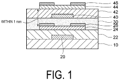
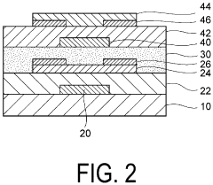
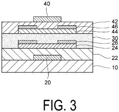
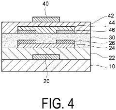
- An inorganic/organic hybrid complementary semiconductor device is developed, featuring a substrate with a p-type organic semiconductor single crystal layer, an n-type amorphous metal oxide inorganic semiconductor layer, and a protective layer, where the p-type organic semiconductor single crystal layer overlaps or does not overlap the n-type amorphous metal oxide layer, with a specific oxygen defect distribution and a distance of 1 mm or less between them, allowing for low-cost manufacturing without the need for high vacuum processes.
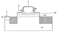
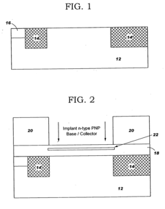
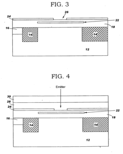
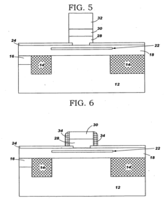
High performance integrated vertical transistors and method of making the same
PatentInactiveUS20070001264A1
Innovation
- The use of a shared silicon germanium (SiGe) low temperature epitaxial (LTE) layer allows for the fabrication of vertically aligned complementary bipolar transistors, where the NPN and PNP transistors share the same epitaxial base and collector regions, with the PNP emitter layer acting as the NPN base layer, utilizing advanced epitaxial techniques like molecular beam epitaxy (MBE) and low temperature epitaxy (LTE) to ensure identical vertical profiles.
Energy Efficiency Considerations in IoT PNP Transistors
Energy efficiency is a critical consideration in the integration of PNP transistors in IoT devices. As these devices often operate on limited power sources, such as batteries or energy harvesting systems, optimizing the energy consumption of transistors becomes paramount. PNP transistors, when properly designed and implemented, can contribute significantly to reducing overall power consumption in IoT applications.
One of the primary approaches to enhancing energy efficiency in PNP transistors for IoT devices is through the optimization of the transistor's structure and materials. Advanced semiconductor materials and fabrication techniques allow for the creation of PNP transistors with lower leakage currents and improved switching characteristics. These improvements directly translate to reduced power consumption during both active and standby modes of operation.
The scaling of transistor dimensions also plays a crucial role in energy efficiency. As transistors become smaller, their power consumption generally decreases. However, this scaling must be carefully balanced with other performance parameters to ensure optimal functionality in IoT applications. Researchers and manufacturers are continually exploring novel transistor architectures that can maintain or improve performance while reducing energy consumption.
Another important aspect of energy efficiency in PNP transistors for IoT devices is the implementation of advanced power management techniques. This includes the use of dynamic voltage and frequency scaling (DVFS), which allows the transistor's operating parameters to be adjusted based on the current workload. By reducing voltage and frequency during periods of low activity, significant power savings can be achieved without compromising overall device performance.
The integration of PNP transistors with other low-power components and circuits is also crucial for maximizing energy efficiency in IoT devices. This holistic approach to system design ensures that the energy-saving benefits of optimized PNP transistors are not negated by inefficiencies in other parts of the device. Techniques such as power gating, where unused sections of the circuit are completely shut down, can further enhance overall energy efficiency.
Emerging technologies, such as tunnel field-effect transistors (TFETs) and negative capacitance field-effect transistors (NCFETs), are being explored as potential alternatives or complements to traditional PNP transistors in IoT applications. These novel transistor types promise even lower power consumption and could revolutionize energy efficiency in future IoT devices.
As IoT devices continue to proliferate and their applications become more diverse, the demand for energy-efficient PNP transistors will only increase. Ongoing research and development efforts are focused on pushing the boundaries of transistor technology to meet these evolving needs, ensuring that IoT devices can operate longer and more efficiently on limited power resources.
Miniaturization Trends in IoT PNP Transistor Design
The miniaturization of PNP transistors in IoT devices has been a significant trend in recent years, driven by the need for more compact, energy-efficient, and cost-effective solutions. This trend has led to several key developments in transistor design and manufacturing processes.
One of the primary focuses has been on reducing the overall size of PNP transistors while maintaining or improving their performance characteristics. This has been achieved through advancements in semiconductor fabrication techniques, such as the use of advanced lithography processes and the development of new materials.
The adoption of silicon-on-insulator (SOI) technology has played a crucial role in miniaturization efforts. SOI allows for better isolation between transistors, reducing parasitic capacitance and enabling higher integration densities. This technology has been particularly beneficial for IoT applications, where power efficiency is paramount.
Another important aspect of miniaturization has been the optimization of transistor structures. Vertical PNP transistors have gained popularity in IoT devices due to their compact footprint and improved high-frequency performance. These structures allow for more efficient use of chip area, enabling higher levels of integration.
The development of advanced packaging technologies has also contributed to the overall miniaturization of IoT devices incorporating PNP transistors. Techniques such as wafer-level packaging and 3D integration have allowed for more compact and efficient device designs, further reducing the size of IoT products.
Researchers and manufacturers have been exploring novel materials to enhance PNP transistor performance while reducing size. For instance, the use of III-V compound semiconductors, such as gallium arsenide (GaAs) and indium phosphide (InP), has shown promise in creating smaller, faster, and more efficient transistors for IoT applications.
The push for miniaturization has also led to innovations in circuit design techniques. Engineers are developing new ways to optimize transistor layouts and interconnects, minimizing the overall chip area required for IoT devices. This includes the use of advanced design automation tools and AI-assisted layout optimization.
As the IoT market continues to grow and diversify, the demand for even smaller and more efficient PNP transistors is expected to increase. Future developments in this area may include the exploration of novel transistor architectures, such as tunnel field-effect transistors (TFETs) or nanowire-based devices, which could potentially offer further size reductions and performance improvements.
Unlock deeper insights with PatSnap Eureka Quick Research — get a full tech report to explore trends and direct your research. Try now!
Generate Your Research Report Instantly with AI Agent
Supercharge your innovation with PatSnap Eureka AI Agent Platform!