Trends in PNP Transistor Reverse Breakdown Voltage Enhancement
JUL 28, 20259 MIN READ
Generate Your Research Report Instantly with AI Agent
Patsnap Eureka helps you evaluate technical feasibility & market potential.
PNP Transistor Evolution
The evolution of PNP transistors has been a significant journey in the field of semiconductor technology. Initially developed in the early 1950s, PNP transistors have undergone numerous improvements and refinements over the decades, particularly in terms of their reverse breakdown voltage capabilities.
In the 1960s and 1970s, the focus was primarily on increasing the overall performance and reliability of PNP transistors. During this period, manufacturers concentrated on improving the doping profiles and junction formations to enhance the transistor's characteristics, including its reverse breakdown voltage.
The 1980s saw a shift towards miniaturization and integration. As the demand for smaller electronic devices grew, researchers worked on scaling down PNP transistors while maintaining or improving their electrical properties. This era marked the beginning of more sophisticated fabrication techniques, which allowed for better control over the transistor's structure and, consequently, its reverse breakdown voltage.
The 1990s brought about significant advancements in semiconductor materials and processing technologies. These developments enabled the creation of PNP transistors with higher reverse breakdown voltages, making them suitable for a wider range of applications, particularly in power electronics and high-voltage circuits.
In the early 2000s, the focus shifted towards optimizing the transistor's architecture. Researchers explored various structural modifications, such as the introduction of guard rings and field plates, to enhance the reverse breakdown voltage without compromising other performance parameters.
The past decade has seen a renewed interest in PNP transistors, driven by the growing demand for high-voltage and high-power applications in sectors like automotive, industrial automation, and renewable energy. This has led to the development of advanced PNP transistors with significantly improved reverse breakdown voltages, often exceeding 100V in some specialized designs.
Recent trends in PNP transistor evolution have focused on leveraging novel materials and innovative fabrication techniques. The use of wide-bandgap semiconductors, such as silicon carbide (SiC) and gallium nitride (GaN), has opened up new possibilities for creating PNP transistors with exceptionally high reverse breakdown voltages, sometimes reaching several hundred volts.
Furthermore, the integration of PNP transistors into more complex power management integrated circuits (PMICs) has driven research towards optimizing their performance within these systems. This has led to the development of PNP transistors with carefully tailored characteristics, balancing high reverse breakdown voltages with other critical parameters such as switching speed and power efficiency.
Market Demand Analysis
The market demand for PNP transistors with enhanced reverse breakdown voltage has been steadily increasing across various industries. This growth is primarily driven by the expanding applications in power electronics, automotive systems, and industrial control equipment. As electronic devices become more compact and energy-efficient, there is a growing need for transistors that can handle higher voltages in smaller packages.
In the automotive sector, the shift towards electric and hybrid vehicles has created a significant demand for high-voltage PNP transistors. These components are crucial in battery management systems, motor controllers, and power distribution units. The automotive industry's stringent reliability requirements and the need for components that can operate in harsh environments further emphasize the importance of enhanced reverse breakdown voltage in PNP transistors.
The industrial automation and control market also contributes substantially to the demand for improved PNP transistors. As factories and manufacturing processes become more sophisticated, there is an increased need for robust transistors that can handle higher voltages in motor drives, programmable logic controllers, and power supplies. The trend towards Industry 4.0 and smart manufacturing is expected to further boost this demand in the coming years.
Consumer electronics represent another significant market segment driving the need for PNP transistors with higher reverse breakdown voltages. With the proliferation of fast-charging technologies and high-power portable devices, there is a growing requirement for transistors that can efficiently manage higher voltages while maintaining compact form factors. This trend is particularly evident in smartphones, laptops, and other mobile devices where space is at a premium.
The renewable energy sector, particularly in solar and wind power systems, is emerging as a key market for enhanced PNP transistors. These components play a critical role in power inverters and converters, where high voltage handling capability is essential for efficient energy conversion and grid integration. As the adoption of renewable energy sources continues to grow globally, the demand for high-performance PNP transistors is expected to rise correspondingly.
In the telecommunications industry, the ongoing rollout of 5G networks and the expansion of data centers are creating new opportunities for PNP transistors with improved reverse breakdown voltages. These components are vital in power amplifiers, base station equipment, and high-speed data transmission systems where reliability and performance under high-voltage conditions are paramount.
The market trend indicates a shift towards more specialized and application-specific PNP transistors. Manufacturers are increasingly focusing on developing customized solutions that meet the unique requirements of different industries, rather than offering generic components. This trend is likely to drive innovation in PNP transistor design and manufacturing processes, leading to further improvements in reverse breakdown voltage capabilities.
Current Challenges
The enhancement of reverse breakdown voltage in PNP transistors faces several significant challenges in the current technological landscape. One of the primary obstacles is the inherent trade-off between breakdown voltage and other critical parameters, such as on-resistance and switching speed. As designers strive to increase the breakdown voltage, they often encounter a corresponding increase in on-resistance, which can negatively impact the overall performance of the transistor.
Another challenge lies in the management of electric field distribution within the device structure. High electric fields at the edges of the transistor can lead to premature breakdown, limiting the achievable reverse breakdown voltage. Developing effective edge termination techniques that can uniformly distribute the electric field remains a complex task, especially as device dimensions continue to shrink.
The scaling of semiconductor devices presents additional hurdles in enhancing reverse breakdown voltage. As transistors become smaller, maintaining high breakdown voltages becomes increasingly difficult due to the reduced physical separation between regions of different doping concentrations. This scaling challenge is particularly pronounced in advanced process nodes, where the room for implementing voltage-enhancing structures is limited.
Material limitations also pose significant constraints on further improvements. While wide-bandgap semiconductors like silicon carbide (SiC) and gallium nitride (GaN) offer promising alternatives for high-voltage applications, integrating these materials into existing silicon-based processes presents considerable technical and economic challenges. The development of cost-effective and reliable fabrication techniques for these advanced materials remains an ongoing area of research.
Furthermore, the demand for higher operating temperatures in various applications, such as automotive and industrial sectors, adds another layer of complexity. Ensuring that PNP transistors maintain their enhanced reverse breakdown voltage characteristics under elevated temperature conditions requires innovative design approaches and potentially new materials that can withstand these harsh environments.
Lastly, the increasing emphasis on energy efficiency and power density in electronic systems places additional pressure on transistor design. Balancing the need for higher breakdown voltages with requirements for lower power consumption and smaller form factors presents a multifaceted challenge that requires holistic optimization of device structure, materials, and fabrication processes.
Existing Enhancement
01 Design considerations for PNP transistor reverse breakdown voltage
The reverse breakdown voltage of PNP transistors is a critical parameter in circuit design. It is influenced by factors such as doping concentrations, junction depths, and device geometry. Proper design considerations can help optimize the reverse breakdown voltage, enhancing the overall performance and reliability of the transistor.- Reverse breakdown voltage enhancement techniques: Various methods are employed to enhance the reverse breakdown voltage of PNP transistors. These techniques include optimizing the doping profile, implementing guard rings, and using specific semiconductor materials. By carefully controlling these factors, the reverse breakdown voltage can be significantly increased, improving the overall performance and reliability of the transistor.
- Circuit design for voltage protection: Circuit designs incorporating PNP transistors often include protective measures to prevent reverse breakdown. These designs may involve voltage clamping circuits, current limiting resistors, or specialized feedback loops. Such protective circuits help to ensure that the PNP transistor operates within its safe voltage range, preventing damage from excessive reverse voltages.
- Semiconductor device structures for improved breakdown voltage: Innovative semiconductor device structures are developed to improve the reverse breakdown voltage of PNP transistors. These structures may include specialized layouts, buried layers, or novel junction designs. By optimizing the physical structure of the transistor, higher reverse breakdown voltages can be achieved without compromising other performance parameters.
- Integration of PNP transistors in high-voltage applications: PNP transistors with high reverse breakdown voltages are crucial in various high-voltage applications. These transistors are integrated into power management circuits, voltage regulators, and switching devices. The design and fabrication processes are optimized to ensure that the PNP transistors can withstand the high voltages encountered in these applications while maintaining their performance characteristics.
- Measurement and characterization of reverse breakdown voltage: Accurate measurement and characterization of the reverse breakdown voltage in PNP transistors are essential for quality control and device optimization. Specialized testing equipment and procedures are developed to precisely determine the breakdown voltage. These measurements help in refining manufacturing processes and ensuring that the transistors meet the required specifications for reverse breakdown voltage.
02 Protection circuits for PNP transistors
Protection circuits are essential for preventing damage to PNP transistors due to reverse breakdown. These circuits can include voltage-limiting components, such as Zener diodes or varistors, to clamp the voltage across the transistor. Implementing effective protection strategies can extend the operational range and lifespan of PNP transistors in various applications.Expand Specific Solutions03 Measurement and characterization of reverse breakdown voltage
Accurate measurement and characterization of the reverse breakdown voltage in PNP transistors are crucial for quality control and performance optimization. Specialized test equipment and methodologies are employed to determine the breakdown voltage under various operating conditions. This information is vital for device modeling and circuit design.Expand Specific Solutions04 Improving reverse breakdown voltage through structural modifications
Structural modifications to PNP transistors can significantly improve their reverse breakdown voltage. Techniques such as edge termination, field plate structures, and optimized doping profiles can be employed to enhance the voltage-handling capability of the device. These modifications aim to reduce electric field crowding and improve overall device performance.Expand Specific Solutions05 Applications utilizing high reverse breakdown voltage PNP transistors
PNP transistors with high reverse breakdown voltages find applications in various fields, including power electronics, automotive systems, and industrial control. These transistors are particularly useful in high-voltage switching circuits, voltage regulators, and protection devices. The ability to withstand high reverse voltages makes them suitable for demanding applications where reliability is crucial.Expand Specific Solutions
Key Industry Players
The trends in PNP transistor reverse breakdown voltage enhancement are evolving within a mature semiconductor industry, yet with ongoing innovation potential. The market is substantial, driven by increasing demand for high-performance electronic devices. Technologically, advancements are incremental, with major players like NXP Semiconductors, Texas Instruments, and Infineon Technologies leading research efforts. Universities such as UESTC and Southeast University contribute to fundamental research, while companies like Micron Technology and Intel focus on practical applications. The involvement of diverse players, from established semiconductor giants to specialized firms like Macronix and emerging players in China, indicates a competitive and dynamic landscape in this niche but crucial area of semiconductor technology.
Texas Instruments Incorporated
Technical Solution: Texas Instruments has made significant strides in enhancing PNP transistor reverse breakdown voltage through several innovative approaches. They have developed a proprietary "resurf" (reduced surface field) technology that allows for higher breakdown voltages while maintaining low on-resistance[2]. This technique involves carefully engineered charge balance in the drift region of the transistor. TI has also implemented advanced isolation techniques, such as deep trench isolation, to prevent punch-through effects and increase breakdown voltage in their high-voltage PNP devices[4]. Furthermore, they have explored the use of silicon-on-insulator (SOI) technology for certain high-voltage applications, which provides inherent isolation and allows for higher breakdown voltages[6].
Strengths: Strong expertise in analog and mixed-signal technologies, extensive manufacturing capabilities. Weaknesses: Potential trade-offs between breakdown voltage and other performance parameters, higher costs associated with advanced isolation techniques.
Infineon Technologies AG
Technical Solution: Infineon has developed advanced PNP transistor designs with enhanced reverse breakdown voltage. Their approach involves optimizing the device structure through innovative doping profiles and edge termination techniques. They have implemented a combination of field plate structures and floating guard rings to redistribute the electric field at the device edges, significantly increasing the breakdown voltage[1]. Additionally, Infineon has explored the use of advanced materials such as silicon carbide (SiC) for high-voltage PNP transistors, which inherently offer higher breakdown voltages due to their wide bandgap properties[3]. The company has also focused on improving the trade-off between breakdown voltage and on-state resistance through careful optimization of the drift region doping and thickness[5].
Strengths: Expertise in power semiconductors, advanced materials research, and innovative device structures. Weaknesses: Potentially higher production costs for advanced designs, and the need for specialized manufacturing processes.
Innovative Approaches
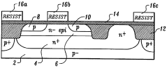
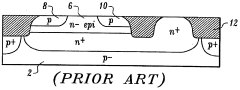
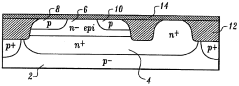
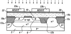
High breakdown lateral PNP transistor
PatentInactiveUS5355015A
Innovation
- An oxide layer is deposited between the N- epitaxial base and the polysilicon layer of the lateral pnp transistor to prevent dopant diffusion, enhancing breakdown voltage characteristics without sacrificing speed advantages.
Power semiconductor device having resurf layer
PatentInactiveEP1267415A3
Innovation
- A semiconductor device with a superjunction structure is developed, where a first drift layer with a lower impurity concentration is integrated between the RESURF layers and the drain layer, allowing for a shared breakdown voltage and reduced ON resistance, and a manufacturing method that forms RESURF layers on the trench walls to ensure uniform depth and crystallinity.


Material Advancements
Material advancements have played a crucial role in enhancing the reverse breakdown voltage of PNP transistors. The continuous pursuit of higher performance and reliability in semiconductor devices has driven significant research and development efforts in this area. One of the key material innovations has been the introduction of advanced epitaxial layers with optimized doping profiles.
These epitaxial layers, typically grown using chemical vapor deposition (CVD) techniques, allow for precise control of impurity concentrations and distributions within the transistor structure. By carefully tailoring the doping gradients, researchers have been able to create more uniform electric field distributions, effectively reducing peak field intensities and increasing the overall breakdown voltage.
Another important material advancement has been the incorporation of wide-bandgap semiconductors, such as silicon carbide (SiC) and gallium nitride (GaN), into PNP transistor designs. These materials offer inherently higher breakdown field strengths compared to traditional silicon, enabling transistors to withstand significantly higher voltages before breakdown occurs.
The use of advanced dielectric materials has also contributed to improved reverse breakdown voltages. High-k dielectrics, such as hafnium oxide (HfO2) and zirconium oxide (ZrO2), have been employed to enhance the gate insulation properties. These materials provide better electrostatic control and reduced leakage currents, indirectly supporting higher breakdown voltages by maintaining better overall device characteristics.
Surface passivation techniques have seen substantial improvements through the development of novel materials and deposition methods. Advanced passivation layers, often consisting of silicon nitride (Si3N4) or aluminum oxide (Al2O3), help to minimize surface states and reduce edge effects that can lead to premature breakdown. These materials are typically deposited using atomic layer deposition (ALD) or plasma-enhanced chemical vapor deposition (PECVD) for precise thickness control and excellent conformality.
The introduction of strain engineering through the use of materials with different lattice constants has also contributed to enhancing reverse breakdown voltages. By inducing controlled strain in the semiconductor lattice, researchers have been able to modify the band structure and carrier mobilities, leading to improved electrical characteristics and higher breakdown voltages.
Recent advancements in nanomaterials and two-dimensional (2D) materials, such as graphene and transition metal dichalcogenides (TMDs), have opened up new possibilities for PNP transistor design. These materials offer unique electronic properties that can be leveraged to create novel device architectures with potentially higher breakdown voltages and improved overall performance.
Reliability Assessment
Reliability assessment is a critical aspect of PNP transistor reverse breakdown voltage enhancement. As the demand for higher voltage ratings and improved performance in power electronics continues to grow, ensuring the long-term reliability of these enhanced transistors becomes paramount. The reliability of PNP transistors with enhanced reverse breakdown voltage is influenced by various factors, including the manufacturing process, materials used, and operating conditions.
One of the primary concerns in reliability assessment is the stability of the enhanced breakdown voltage over time. Accelerated aging tests are commonly employed to evaluate the long-term performance of these transistors. These tests subject the devices to elevated temperatures, high voltages, and other stress conditions to simulate years of operation in a compressed timeframe. The results of these tests provide valuable insights into the degradation mechanisms and potential failure modes of the enhanced PNP transistors.
Another crucial aspect of reliability assessment is the evaluation of the transistor's robustness under different operating conditions. This includes testing the device's performance across a wide range of temperatures, voltages, and current levels. The goal is to ensure that the enhanced reverse breakdown voltage remains stable and effective under various real-world scenarios. Additionally, the impact of environmental factors such as humidity and electromagnetic interference on the transistor's reliability is thoroughly examined.
The reliability of the enhanced PNP transistors is also closely tied to the manufacturing process. Quality control measures and process optimization play a significant role in ensuring consistent and reliable performance. Advanced inspection techniques, such as electron microscopy and spectroscopic analysis, are employed to detect potential defects or irregularities in the transistor structure that could compromise its reliability.
Furthermore, reliability assessment involves the analysis of failure modes and mechanisms specific to enhanced reverse breakdown voltage transistors. This includes investigating phenomena such as hot carrier injection, time-dependent dielectric breakdown, and electromigration. Understanding these failure mechanisms allows for the development of mitigation strategies and design improvements to enhance the overall reliability of the transistors.
Statistical analysis and modeling techniques are extensively used in reliability assessment to predict the long-term performance and lifetime of enhanced PNP transistors. These models take into account various factors, including operating conditions, environmental stresses, and manufacturing variations, to provide accurate estimates of the device's reliability metrics, such as mean time between failures (MTBF) and failure rate.
In conclusion, reliability assessment is an integral part of the development and implementation of PNP transistors with enhanced reverse breakdown voltage. It ensures that these advanced devices can meet the demanding requirements of modern power electronics applications while maintaining long-term stability and performance. The comprehensive approach to reliability assessment, combining accelerated testing, failure analysis, and statistical modeling, provides valuable insights for continuous improvement and optimization of these critical components.
Unlock deeper insights with Patsnap Eureka Quick Research — get a full tech report to explore trends and direct your research. Try now!
Generate Your Research Report Instantly with AI Agent
Supercharge your innovation with Patsnap Eureka AI Agent Platform!