

Utilizing PNP Transistors in Broadband Technology
JUL 28, 202510 MIN READ
Generate Your Research Report Instantly with AI Agent
Patsnap Eureka helps you evaluate technical feasibility & market potential.
PNP Transistors in Broadband: Background and Objectives
PNP transistors have played a crucial role in the evolution of broadband technology, serving as fundamental components in various electronic circuits. The journey of utilizing PNP transistors in broadband applications began in the mid-20th century, following their invention in 1947. As the demand for faster and more efficient communication systems grew, engineers and researchers recognized the potential of PNP transistors in amplifying and processing high-frequency signals.
The development of broadband technology has been driven by the need for increased data transmission rates and wider bandwidth capabilities. PNP transistors, with their ability to control current flow and amplify signals, have been instrumental in achieving these goals. Their unique characteristics, such as low noise, high gain, and excellent frequency response, make them particularly suitable for broadband applications.
Over the years, the integration of PNP transistors in broadband circuits has undergone significant advancements. From early analog systems to modern digital communication networks, these transistors have been continuously optimized to meet the ever-increasing demands of the telecommunications industry. The miniaturization of transistors and the development of advanced manufacturing processes have further enhanced their performance and reliability in broadband applications.
The primary objective of utilizing PNP transistors in broadband technology is to improve the overall efficiency and performance of communication systems. This includes enhancing signal amplification, reducing noise, and increasing bandwidth capacity. By leveraging the unique properties of PNP transistors, engineers aim to develop more compact, energy-efficient, and cost-effective broadband solutions.
Another key goal is to address the challenges posed by the growing demand for high-speed internet and mobile communications. PNP transistors play a vital role in the design of advanced broadband amplifiers, mixers, and oscillators, which are essential components in modern communication systems. The ongoing research and development in this field focus on pushing the boundaries of transistor performance to support emerging technologies such as 5G networks and beyond.
Furthermore, the utilization of PNP transistors in broadband technology aims to improve the overall quality of service for end-users. This includes enhancing signal integrity, reducing latency, and increasing data transmission speeds. As the world becomes increasingly interconnected, the role of PNP transistors in broadband applications continues to evolve, driving innovation in areas such as Internet of Things (IoT), smart cities, and autonomous vehicles.
In conclusion, the background of PNP transistors in broadband technology reflects a rich history of technological advancement and innovation. The objectives for their continued utilization are centered around meeting the growing demands of the digital age, improving communication infrastructure, and enabling new applications that require high-speed, reliable data transmission. As research progresses, the potential of PNP transistors in broadband technology remains a key area of focus for engineers and scientists worldwide.
Market Demand Analysis for Broadband Technologies
The demand for broadband technologies has been experiencing exponential growth in recent years, driven by the increasing need for high-speed internet connectivity across various sectors. The global broadband market is projected to reach significant valuation by 2025, with a compound annual growth rate (CAGR) surpassing industry averages. This growth is primarily fueled by the rising adoption of smart devices, the proliferation of Internet of Things (IoT) applications, and the increasing demand for high-bandwidth services such as video streaming and cloud computing.
In the context of utilizing PNP transistors in broadband technology, the market demand is closely tied to the overall expansion of broadband infrastructure and the need for more efficient and cost-effective solutions. PNP transistors, known for their ability to amplify and switch electronic signals, play a crucial role in various broadband applications, including signal amplification, noise reduction, and power management in broadband circuits.
The telecommunications sector represents a significant portion of the market demand for broadband technologies incorporating PNP transistors. As telecom companies continue to upgrade their networks to support 5G and beyond, there is a growing need for advanced components that can handle higher frequencies and provide better signal integrity. PNP transistors, when optimized for broadband applications, can offer improved performance in terms of bandwidth, linearity, and power efficiency.
Consumer electronics is another key driver of market demand in this space. With the increasing popularity of smart home devices, wearables, and high-definition multimedia systems, there is a rising demand for broadband-capable components that can deliver faster data rates and lower latency. PNP transistors integrated into these devices can enhance their connectivity capabilities and overall performance.
The enterprise sector also contributes significantly to the market demand for broadband technologies. As businesses increasingly rely on cloud services, video conferencing, and data-intensive applications, there is a growing need for robust and reliable broadband infrastructure. PNP transistors can play a vital role in improving the performance and reliability of enterprise-grade networking equipment.
Emerging technologies such as autonomous vehicles, smart cities, and industrial IoT are expected to further drive the demand for advanced broadband solutions. These applications require ultra-reliable and low-latency communication, where PNP transistors can contribute to achieving the necessary performance metrics.
Geographically, the market demand for broadband technologies utilizing PNP transistors varies across regions. Developed markets like North America and Europe show a strong demand for cutting-edge broadband solutions, while emerging markets in Asia-Pacific and Latin America present significant growth opportunities due to ongoing infrastructure development and increasing internet penetration rates.
In conclusion, the market demand for broadband technologies, particularly those leveraging PNP transistors, is robust and multifaceted. The convergence of various technological trends and the increasing reliance on high-speed connectivity across industries are expected to sustain this demand in the foreseeable future.
Current State and Challenges of PNP Transistors in Broadband
PNP transistors have been integral to broadband technology, playing a crucial role in signal amplification and switching. Currently, these transistors are widely used in various broadband applications, including cable modems, fiber-optic networks, and wireless communication systems. The current state of PNP transistors in broadband technology is characterized by continuous improvements in performance, efficiency, and integration capabilities.
One of the primary challenges facing PNP transistors in broadband applications is the need for higher frequency operation. As broadband technologies evolve to support faster data rates and wider bandwidths, transistors must operate at increasingly higher frequencies. This requirement pushes the limits of traditional PNP transistor designs, necessitating innovative approaches to overcome inherent frequency limitations.
Another significant challenge is power consumption. With the growing demand for energy-efficient devices, reducing the power consumption of PNP transistors in broadband circuits has become a critical focus. Researchers and engineers are exploring various techniques to minimize power dissipation while maintaining high performance, including advanced biasing schemes and novel semiconductor materials.
The integration of PNP transistors with other components in broadband circuits presents additional challenges. As circuit densities increase and form factors shrink, designers must address issues related to thermal management, signal integrity, and electromagnetic interference. These factors become particularly crucial in high-frequency broadband applications where parasitic effects can significantly impact performance.
Manufacturability and cost-effectiveness remain ongoing concerns in the development of PNP transistors for broadband technology. The industry continually seeks ways to improve production processes, increase yields, and reduce costs while meeting the demanding specifications required for broadband applications. This challenge is particularly evident in the development of advanced semiconductor processes that can support both high-frequency operation and large-scale integration.
The current state of PNP transistors in broadband technology also reflects a shift towards more specialized designs tailored for specific applications. This trend has led to the development of custom PNP transistor structures optimized for particular frequency ranges, power levels, and noise characteristics. While this approach allows for improved performance in targeted applications, it also presents challenges in terms of design complexity and potential limitations in versatility.
Researchers are actively exploring new materials and device structures to overcome the limitations of traditional silicon-based PNP transistors. Compound semiconductors, such as silicon-germanium (SiGe) and III-V materials, are being investigated for their potential to offer superior high-frequency performance and improved power efficiency in broadband applications. However, integrating these advanced materials into existing manufacturing processes and ensuring their long-term reliability remain significant challenges.
Existing Solutions for PNP Transistor Implementation
01 Structure and fabrication of PNP transistors
PNP transistors are semiconductor devices with specific structures and fabrication methods. They typically consist of a p-type emitter, n-type base, and p-type collector. The manufacturing process involves various steps such as doping, etching, and layering to create the desired transistor structure.- Structure and fabrication of PNP transistors: PNP transistors are semiconductor devices with specific structures and fabrication methods. They typically consist of a p-type emitter, n-type base, and p-type collector. The manufacturing process involves various steps such as doping, etching, and layering to create the desired transistor characteristics.
- Applications of PNP transistors in electronic circuits: PNP transistors are widely used in various electronic circuits for amplification, switching, and signal processing. They are often employed in complementary circuits with NPN transistors, power supplies, and analog circuits. Their unique properties make them suitable for specific applications in electronic design.
- Performance optimization and characteristics: Improving the performance of PNP transistors involves optimizing various parameters such as current gain, switching speed, and power handling capabilities. This can be achieved through careful design of the transistor structure, doping profiles, and manufacturing processes. Understanding and controlling these characteristics is crucial for enhancing overall device performance.
- Integration of PNP transistors in integrated circuits: PNP transistors are often integrated into larger semiconductor devices and integrated circuits. This integration requires careful consideration of layout, interconnections, and compatibility with other components. Techniques for efficient integration and minimizing parasitic effects are essential for optimal performance in complex circuits.
- Testing and characterization of PNP transistors: Accurate testing and characterization of PNP transistors are crucial for quality control and performance verification. This involves measuring various electrical parameters, such as current gain, breakdown voltage, and leakage current. Specialized testing equipment and procedures are used to ensure the reliability and consistency of PNP transistors in different applications.
02 Applications of PNP transistors in electronic circuits
PNP transistors are widely used in various electronic circuits for amplification, switching, and signal processing. They are often employed in complementary circuits with NPN transistors, power supplies, and analog circuits. Their unique characteristics make them suitable for specific applications in electronic design.Expand Specific Solutions03 Performance optimization and characteristics of PNP transistors
Improving the performance of PNP transistors involves optimizing various parameters such as current gain, frequency response, and noise characteristics. This can be achieved through careful design of the transistor structure, doping profiles, and manufacturing processes. Understanding and enhancing these characteristics is crucial for optimal transistor performance in different applications.Expand Specific Solutions04 Integration of PNP transistors in semiconductor devices
PNP transistors are often integrated into larger semiconductor devices and integrated circuits. This integration requires careful consideration of layout, interconnections, and compatibility with other components. Advanced manufacturing techniques are employed to ensure proper functioning of PNP transistors within complex semiconductor structures.Expand Specific Solutions05 Testing and characterization of PNP transistors
Accurate testing and characterization of PNP transistors are essential for quality control and performance verification. Various methods and equipment are used to measure parameters such as current gain, breakdown voltage, and leakage current. These tests ensure the reliability and consistency of PNP transistors in different operating conditions.Expand Specific Solutions
Key Players in PNP Transistor and Broadband Industry
The utilization of PNP transistors in broadband technology is in a mature stage of development, with a significant market size due to the widespread adoption of broadband communications. The technology's maturity is evident from the involvement of established players like IBM, Infineon Technologies, and STMicroelectronics, who have extensive experience in semiconductor manufacturing. These companies, along with others like GLOBALFOUNDRIES and Texas Instruments, are continuously refining PNP transistor technology to improve performance in broadband applications. The competitive landscape is characterized by ongoing innovation and optimization efforts, focusing on enhancing speed, efficiency, and reliability in broadband systems.
International Business Machines Corp.
Technical Solution: IBM has developed advanced PNP transistor designs for broadband applications, focusing on high-frequency performance and low noise. Their technology utilizes Silicon-Germanium (SiGe) heterojunction bipolar transistors (HBTs) to achieve cutoff frequencies exceeding 300 GHz [1]. IBM's approach involves optimizing the base and emitter regions to reduce parasitic capacitances and improve current gain. They have also implemented advanced lithography techniques to achieve sub-100 nm feature sizes, enhancing the transistor's speed and bandwidth capabilities [3]. IBM's PNP transistors incorporate self-aligned structures and precise doping profiles to minimize base resistance and maximize current gain, crucial for broadband applications [5].
Strengths: Industry-leading performance in high-frequency applications, advanced manufacturing capabilities. Weaknesses: Potentially higher production costs, complexity in integration with standard CMOS processes.
Infineon Technologies AG
Technical Solution: Infineon has developed specialized PNP transistors for broadband applications, focusing on high linearity and low noise performance. Their technology utilizes advanced Silicon-Germanium (SiGe) processes to achieve high transition frequencies and low base resistance. Infineon's PNP transistors feature optimized vertical doping profiles and lateral scaling to enhance RF performance [2]. They have implemented innovative emitter and base designs to reduce parasitic capacitances and improve power handling capabilities. Infineon's broadband PNP transistors also incorporate advanced thermal management techniques to ensure stable operation at high frequencies [4].
Strengths: Excellent linearity and noise performance, robust thermal management. Weaknesses: Potentially higher cost compared to standard bipolar transistors, limited to specific application areas.
Core Innovations in PNP Transistor Design for Broadband
Communication method and apparatus
PatentWO2020098145A1
Innovation
- Efficient multi-band access through cross-band frame transmission, enabling seamless communication between 2.4/5.9 GHz and 6 GHz bands.
- Utilization of BSSID or RNR elements for extended frequency range access (1-7 GHz), enhancing flexibility in band usage.
- Implementation of signaling mechanisms to indicate co-located APs and multi-band capabilities, improving network resource allocation.
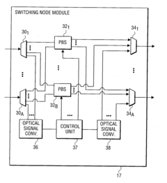
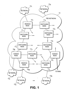
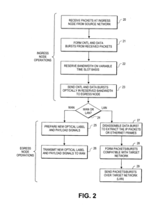
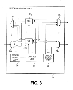
Adaptive framework for closed-loop protocols over photonic burst switched networks
PatentActiveUS20040258407A1
Innovation
- The implementation of a photonic burst-switched (PBS) network that uses optical switching units to route data bursts without O-E-O conversion at switching nodes, employing statistical multiplexing and GMPLS-based architecture for efficient bandwidth management and control signaling.
Frequency Allocation and Regulatory Considerations
The allocation of frequency spectrum for broadband technology utilizing PNP transistors is a critical consideration that involves complex regulatory frameworks and technical constraints. Regulatory bodies such as the Federal Communications Commission (FCC) in the United States and similar organizations worldwide play a crucial role in managing and allocating frequency bands for various applications, including broadband technologies.
In the context of PNP transistors in broadband technology, frequency allocation typically focuses on the ultra-high frequency (UHF) and super-high frequency (SHF) ranges. These bands, spanning from 300 MHz to 30 GHz, are particularly suitable for broadband applications due to their capacity for high data rates and relatively low atmospheric attenuation.
The regulatory landscape for frequency allocation is dynamic and varies across different regions. In recent years, there has been a global trend towards harmonizing frequency allocations to facilitate international roaming and interoperability of broadband devices. This harmonization effort has led to the designation of specific bands for broadband applications, such as the 700 MHz, 2.4 GHz, and 5 GHz bands.
Regulatory considerations for PNP transistor-based broadband technology extend beyond mere frequency allocation. Emission standards, power limits, and interference mitigation requirements are integral parts of the regulatory framework. These regulations aim to ensure efficient spectrum usage, minimize interference between different services, and protect public safety and national security interests.
The implementation of PNP transistors in broadband technology must adhere to these regulatory standards. This includes compliance with specific technical parameters such as out-of-band emissions, spurious emissions, and power spectral density limits. Manufacturers and service providers must obtain necessary certifications and approvals from regulatory bodies before deploying their technologies.
Furthermore, the regulatory landscape is evolving to accommodate emerging technologies and increasing demand for spectrum. Concepts such as dynamic spectrum access, cognitive radio, and spectrum sharing are gaining traction, potentially offering new opportunities for PNP transistor-based broadband systems to operate more efficiently within the allocated frequency bands.
As the demand for broadband services continues to grow, regulators face the challenge of balancing the needs of various stakeholders while ensuring optimal spectrum utilization. This often involves reallocating spectrum from legacy services to new broadband applications, a process known as spectrum refarming. The successful integration of PNP transistor technology in broadband systems will depend on navigating these regulatory complexities and adapting to evolving frequency allocation frameworks.
Environmental Impact of PNP Transistor Manufacturing
The manufacturing process of PNP transistors, while essential for broadband technology, carries significant environmental implications. The production of these semiconductor devices involves several stages, each with its own ecological footprint. The primary environmental concerns stem from the use of hazardous materials, energy consumption, and waste generation.
Raw material extraction and processing constitute the initial phase of environmental impact. Silicon, the base material for transistors, is typically obtained through mining and refining processes that can lead to habitat disruption and air pollution. The purification of silicon to semiconductor-grade quality requires substantial energy input, contributing to greenhouse gas emissions.
The fabrication of PNP transistors involves complex chemical processes, including doping, etching, and photolithography. These processes utilize a range of chemicals, some of which are highly toxic or corrosive. Chemicals such as hydrofluoric acid, sulfuric acid, and various solvents pose risks of soil and water contamination if not properly managed. Additionally, the production of ultra-pure water, essential for semiconductor manufacturing, demands significant energy and water resources.
Cleanroom operations, necessary for maintaining the sterile environment required in transistor production, consume large amounts of energy for air filtration, temperature, and humidity control. The constant operation of these facilities contributes to the industry's overall carbon footprint.
Waste management presents another critical environmental challenge. The semiconductor industry generates various types of waste, including hazardous chemicals, contaminated water, and discarded silicon wafers. Proper treatment and disposal of these materials are essential to prevent environmental contamination and comply with regulatory standards.
The use of rare earth elements in certain transistor components adds another layer of environmental concern. The mining and processing of these elements often involve environmentally destructive practices and can lead to soil degradation and water pollution in mining regions.
As the demand for broadband technology grows, the environmental impact of PNP transistor manufacturing is likely to increase. However, the industry is making strides towards more sustainable practices. Efforts include developing more energy-efficient manufacturing processes, implementing closed-loop water recycling systems, and exploring alternative materials with lower environmental impacts.
Regulatory bodies worldwide are imposing stricter environmental standards on semiconductor manufacturing, driving innovation in cleaner production methods. Companies are increasingly adopting life cycle assessment approaches to evaluate and mitigate the environmental impacts of their products from cradle to grave.
Unlock deeper insights with Patsnap Eureka Quick Research — get a full tech report to explore trends and direct your research. Try now!
Generate Your Research Report Instantly with AI Agent
Supercharge your innovation with Patsnap Eureka AI Agent Platform!