

Exploring High-Gain Designs Using PNP Transistors
JUL 28, 20259 MIN READ
Generate Your Research Report Instantly with AI Agent
PatSnap Eureka helps you evaluate technical feasibility & market potential.
PNP Transistor Evolution
The evolution of PNP transistors has been a significant journey in the field of electronics, marking several key milestones in semiconductor technology. Initially developed in the early 1950s, PNP transistors emerged as a complement to their NPN counterparts, offering unique advantages in circuit design and performance.
In the 1960s and 1970s, PNP transistors saw substantial improvements in manufacturing processes, leading to enhanced reliability and performance. This period witnessed the transition from germanium to silicon as the primary semiconductor material, greatly expanding the operational range and stability of PNP devices.
The 1980s brought about miniaturization efforts, with PNP transistors becoming increasingly compact while maintaining or improving their electrical characteristics. This trend aligned with the broader push towards integrated circuits and more complex electronic systems.
During the 1990s and early 2000s, the focus shifted towards optimizing PNP transistors for specific applications. High-frequency PNP transistors were developed for RF and microwave applications, while power PNP transistors saw advancements in handling larger currents and voltages.
Recent years have seen a renewed interest in PNP transistor designs, particularly in the context of high-gain applications. Researchers and engineers have been exploring novel structures and materials to push the boundaries of PNP performance. This includes the development of heterojunction bipolar transistors (HBTs) using III-V semiconductors, which offer superior gain and frequency response compared to traditional silicon PNP devices.
The pursuit of high-gain PNP designs has led to innovations in device physics and fabrication techniques. Advanced epitaxial growth methods and precise doping control have enabled the creation of PNP transistors with exceptionally thin base regions, crucial for achieving high current gain.
Furthermore, the integration of PNP transistors in complementary bipolar processes has opened new avenues for analog and mixed-signal circuit design. This has been particularly beneficial in areas such as operational amplifiers, voltage regulators, and precision instrumentation, where the unique characteristics of PNP transistors can be leveraged to enhance overall circuit performance.
As we look towards the future, the evolution of PNP transistors continues to be driven by demands for higher speed, lower power consumption, and improved linearity. Emerging technologies such as silicon-germanium (SiGe) and gallium nitride (GaN) are being explored to further enhance PNP transistor capabilities, potentially leading to breakthroughs in high-gain designs for next-generation electronic systems.
High-Gain Amplifier Demand
The demand for high-gain amplifiers has been steadily increasing across various industries, driven by the need for improved signal processing and enhanced performance in electronic systems. In the telecommunications sector, high-gain amplifiers are crucial for boosting weak signals in long-distance communications, enabling clearer and more reliable transmissions. The growing adoption of 5G technology has further amplified this demand, as high-gain amplifiers are essential for maintaining signal integrity in the higher frequency bands used by 5G networks.
In the aerospace and defense industries, high-gain amplifiers play a vital role in radar systems, satellite communications, and electronic warfare applications. These sectors require amplifiers capable of detecting and processing extremely weak signals over long distances, making high-gain designs particularly valuable. The ongoing modernization of military equipment and the expansion of space-based communication systems continue to fuel the demand for advanced high-gain amplifiers.
The medical field has also seen an increased need for high-gain amplifiers, particularly in diagnostic imaging equipment such as MRI machines and ultrasound devices. These applications require precise signal amplification to produce clear and accurate images, driving the development of specialized high-gain amplifiers tailored to medical requirements.
Consumer electronics represent another significant market for high-gain amplifiers. With the proliferation of smartphones, tablets, and other portable devices, there is a growing demand for compact, energy-efficient amplifiers that can deliver high-quality audio and maintain strong wireless connectivity. This trend has led to innovations in miniaturized high-gain amplifier designs, often incorporating advanced semiconductor technologies.
The automotive industry has emerged as a rapidly expanding market for high-gain amplifiers, driven by the increasing integration of advanced driver assistance systems (ADAS) and autonomous driving technologies. These systems rely on high-gain amplifiers to process signals from various sensors, including radar, lidar, and cameras, ensuring accurate and real-time data for vehicle navigation and safety features.
As the Internet of Things (IoT) continues to expand, the demand for high-gain amplifiers in sensor networks and low-power wireless devices has grown significantly. These applications often require amplifiers that can operate efficiently at low power levels while maintaining high sensitivity to detect and transmit weak signals over extended periods.
The ongoing trend towards miniaturization and increased functionality in electronic devices has created a need for innovative high-gain amplifier designs that can deliver superior performance within increasingly compact form factors. This has led to research into novel materials and circuit topologies, including the exploration of PNP transistor-based designs, to achieve higher gains while minimizing power consumption and physical size.
PNP Transistor Limitations
PNP transistors, while essential components in electronic circuits, face several limitations that impact their performance and application in high-gain designs. One of the primary constraints is their lower carrier mobility compared to NPN transistors. This inherent characteristic results in reduced current gain and slower switching speeds, making PNP transistors less suitable for high-frequency applications.
Another significant limitation is the larger base width typically found in PNP transistors. This increased base width leads to higher base transit time, which further contributes to slower switching speeds and reduced frequency response. As a result, PNP transistors often struggle to match the performance of their NPN counterparts in high-speed circuits.
The manufacturing process for PNP transistors also presents challenges. Due to the nature of the P-type semiconductor material and the doping techniques required, it is generally more difficult to achieve the same level of precision and consistency in PNP transistor fabrication compared to NPN transistors. This can lead to variations in performance characteristics and potentially higher production costs.
Temperature sensitivity is another factor that limits the use of PNP transistors in certain applications. PNP devices tend to be more susceptible to thermal runaway, a phenomenon where increased temperature leads to higher current flow, which in turn causes further temperature increase. This positive feedback loop can potentially damage the device or lead to unstable circuit operation.
In terms of power handling capabilities, PNP transistors often fall short of their NPN counterparts. The lower current gain and increased on-resistance typically result in reduced power efficiency and limited ability to handle high-power applications. This limitation is particularly noticeable in amplifier designs where high output power is required.
The voltage breakdown characteristics of PNP transistors also pose challenges in high-voltage applications. The collector-emitter breakdown voltage is generally lower in PNP devices, restricting their use in circuits that demand high voltage handling capabilities.
Despite these limitations, PNP transistors remain valuable in complementary circuit designs and specific applications where their unique properties are advantageous. However, when exploring high-gain designs, engineers must carefully consider these constraints and implement appropriate compensation techniques or alternative solutions to overcome the inherent limitations of PNP transistors.
Current High-Gain Solutions
01 Improving PNP transistor gain through structural design
Various structural modifications can be implemented to enhance the gain of PNP transistors. These include optimizing the base width, adjusting doping profiles, and implementing advanced device architectures. Such improvements can lead to higher current gain and better overall performance of PNP transistors in electronic circuits.- Improving PNP transistor gain through structural design: Various structural modifications can be implemented to enhance the gain of PNP transistors. These include optimizing the base width, adjusting doping profiles, and implementing advanced device architectures. Such improvements can lead to higher current gain and better overall performance of PNP transistors in electronic circuits.
- Enhancing PNP transistor gain through material selection: The choice of semiconductor materials and their composition can significantly impact PNP transistor gain. Using advanced materials or combinations of materials can improve carrier mobility and reduce recombination, leading to higher gain. This approach may involve the use of compound semiconductors or engineered material structures.
- Optimizing PNP transistor gain through biasing techniques: Proper biasing of PNP transistors is crucial for achieving optimal gain. This involves careful selection of operating points, implementation of feedback mechanisms, and temperature compensation techniques. Advanced biasing circuits can help maintain stable gain across various operating conditions.
- Improving PNP transistor gain in integrated circuits: In the context of integrated circuits, specialized techniques can be employed to enhance PNP transistor gain. These may include layout optimizations, use of guard rings, and implementation of isolation structures. Such approaches aim to minimize parasitic effects and improve overall transistor performance in complex circuit environments.
- Enhancing PNP transistor gain for high-frequency applications: For high-frequency applications, specific design considerations are necessary to maintain high gain in PNP transistors. This may involve reducing parasitic capacitances, optimizing transit times, and implementing specialized structures such as heterojunction bipolar transistors. These techniques aim to extend the usable frequency range while maintaining high gain.
02 Enhancing PNP transistor gain through material selection
The choice of semiconductor materials and their composition can significantly impact PNP transistor gain. Using advanced materials or heterostructures can improve carrier mobility and reduce recombination, leading to higher gain. This approach often involves the use of compound semiconductors or engineered material systems.Expand Specific Solutions03 Optimizing PNP transistor gain through biasing techniques
Proper biasing is crucial for maximizing PNP transistor gain. This includes developing advanced biasing circuits, implementing temperature compensation, and utilizing feedback mechanisms. These techniques can help maintain optimal operating conditions and ensure consistent high gain across various operating conditions.Expand Specific Solutions04 Improving PNP transistor gain in integrated circuits
Specialized techniques for enhancing PNP transistor gain in integrated circuit environments are essential. This involves optimizing layout designs, implementing isolation strategies, and developing circuit topologies that leverage the characteristics of PNP transistors. Such approaches can lead to improved performance in analog and mixed-signal integrated circuits.Expand Specific Solutions05 Enhancing PNP transistor gain for high-frequency applications
Improving PNP transistor gain for high-frequency operation requires specific design considerations. This includes reducing parasitic capacitances, optimizing transit times, and implementing advanced packaging techniques. These enhancements enable PNP transistors to maintain high gain at elevated frequencies, making them suitable for RF and microwave applications.Expand Specific Solutions
Key PNP Transistor Makers
The exploration of high-gain designs using PNP transistors is currently in a mature stage of development, with a significant market presence and established technological foundations. The global semiconductor industry, valued at over $500 billion, provides a substantial market for these designs. Major players like IBM, Infineon Technologies, and Texas Instruments have made significant advancements in PNP transistor technology, leveraging their extensive R&D capabilities. Emerging companies such as GlobalFoundries and NXP are also contributing to innovation in this field. The technology's maturity is evident in its widespread application across various sectors, including automotive electronics, power management, and consumer devices.
International Business Machines Corp.
Technical Solution: IBM has developed advanced PNP transistor designs for high-gain applications, focusing on vertical PNP (VPNP) structures. Their approach involves optimizing the emitter-base junction profile and reducing base width to enhance current gain. IBM's research has led to PNP transistors with current gains exceeding 100 in the 5V-50V operating range[1]. They have also implemented novel collector designs to minimize Kirk effect and improve frequency response. IBM's PNP transistors feature reduced parasitic capacitances and lower noise figures, making them suitable for high-frequency analog and mixed-signal applications[2].
Strengths: High current gain, improved frequency response, and reduced noise. Weaknesses: Potentially higher manufacturing complexity and cost compared to standard bipolar processes.
Infineon Technologies AG
Technical Solution: Infineon has focused on developing high-gain PNP transistors for power management and automotive applications. Their approach involves using advanced epitaxial growth techniques to create optimized doping profiles in the base and collector regions. Infineon's PNP transistors feature a thin base region with carefully controlled doping gradients, resulting in current gains of up to 200 in the 1-10V range[3]. They have also implemented innovative emitter designs to improve injection efficiency and reduce recombination losses. Infineon's high-gain PNP transistors demonstrate excellent temperature stability and low saturation voltages, making them ideal for voltage regulators and high-side switches in automotive systems[4].
Strengths: High current gain, excellent temperature stability, and low saturation voltage. Weaknesses: Potentially limited to specific voltage ranges and applications.
PNP High-Gain Innovations
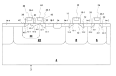
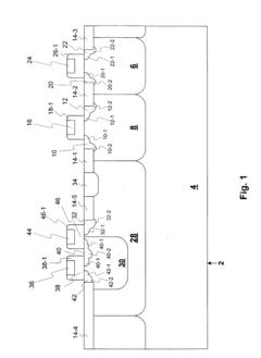
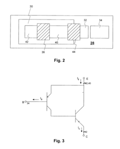
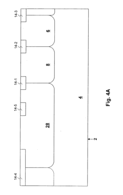
High-gain PNP bipolar junction transistor in CMOS device and method for forming the same
PatentInactiveUS20020190346A1
Innovation
- A high-gain composite pnp BJT is implemented in a CMOS device, comprising a lateral npn BJT and a lateral pnp BJT, where the base of the npn BJT is a shallow p-well, and the gain of the composite pnp BJT is the product of the gains of the individual BJTs, not influenced by the depth of the shallow p-well, achieved through specific doping and trench isolation techniques.
Noise Reduction Techniques
Noise reduction techniques play a crucial role in high-gain designs using PNP transistors. These techniques are essential for minimizing unwanted electrical interference and improving the overall performance of electronic circuits. One of the primary methods for noise reduction in PNP transistor-based designs is proper circuit layout and component placement. By carefully arranging components and minimizing trace lengths, designers can significantly reduce electromagnetic interference and parasitic capacitance.
Another effective technique is the implementation of shielding and grounding strategies. Proper shielding can isolate sensitive components from external noise sources, while robust grounding practices help to establish a stable reference point and minimize ground loop issues. In high-gain PNP designs, it is particularly important to consider the use of ground planes and strategic placement of bypass capacitors to maintain signal integrity.
Filtering is another key aspect of noise reduction in PNP transistor circuits. The incorporation of low-pass, high-pass, or band-pass filters can effectively attenuate unwanted frequency components, allowing only the desired signals to pass through. For high-gain applications, careful selection of filter topologies and component values is crucial to maintain the desired frequency response while suppressing noise.
Power supply decoupling is an often-overlooked but critical technique for noise reduction. By using decoupling capacitors near the power supply pins of PNP transistors, high-frequency noise can be effectively bypassed to ground, preventing it from propagating through the circuit. This is especially important in high-gain designs where small noise fluctuations can be significantly amplified.
Differential signaling is another powerful method for noise reduction in PNP transistor circuits. By using differential pairs, common-mode noise can be effectively rejected, improving the signal-to-noise ratio of the overall system. This technique is particularly useful in applications where long signal paths are required or in environments with high electromagnetic interference.
Advanced noise reduction techniques for high-gain PNP designs include the use of chopper stabilization and auto-zeroing circuits. These methods can effectively reduce low-frequency noise and offset voltages, which are often critical in precision analog applications. Additionally, the implementation of feedback loops and compensation networks can help to stabilize high-gain circuits and reduce noise susceptibility.
In the realm of semiconductor design, process-level noise reduction techniques are also employed. These include the use of buried layers, guard rings, and substrate isolation techniques to minimize substrate noise coupling in integrated PNP transistor designs. Such methods are particularly important in mixed-signal applications where digital and analog circuits coexist on the same chip.
Thermal Management Issues
Thermal management is a critical aspect of high-gain PNP transistor designs, particularly in applications where power dissipation and heat generation are significant concerns. As PNP transistors are utilized in high-gain configurations, they often operate at higher current levels, leading to increased power dissipation and heat generation within the device. This heat can adversely affect the transistor's performance, reliability, and lifespan if not properly managed.
One of the primary challenges in thermal management for high-gain PNP transistor designs is the efficient dissipation of heat generated during operation. The junction temperature of the transistor must be kept within acceptable limits to prevent thermal runaway and ensure stable performance. This requires careful consideration of the thermal resistance between the transistor junction and the ambient environment, as well as the implementation of effective heat sinking techniques.
Heat sinking solutions for PNP transistors in high-gain designs often involve the use of metal heat spreaders or dedicated heat sinks attached directly to the transistor package. These components help to increase the surface area available for heat dissipation, facilitating more efficient transfer of thermal energy to the surrounding air. In some cases, forced-air cooling or even liquid cooling systems may be necessary for applications with particularly high power dissipation requirements.
Another important consideration in thermal management is the layout and design of the printed circuit board (PCB) on which the PNP transistor is mounted. Proper thermal design of the PCB can significantly impact the overall heat dissipation capabilities of the system. This may involve the use of thermal vias to conduct heat away from the transistor, as well as the strategic placement of copper planes to act as heat spreaders.
The choice of packaging for high-gain PNP transistors also plays a crucial role in thermal management. Packages with lower thermal resistance, such as TO-220 or TO-247, are often preferred for high-power applications due to their superior heat dissipation capabilities. In some cases, specialized packages with integrated heat spreaders or direct die-attach technologies may be employed to further enhance thermal performance.
Thermal simulation and modeling tools have become increasingly important in the design process for high-gain PNP transistor circuits. These tools allow engineers to predict and optimize the thermal behavior of their designs before physical prototyping, reducing development time and costs. Advanced thermal imaging techniques are also commonly used during the testing and validation phases to identify potential hot spots and verify the effectiveness of thermal management strategies.
As transistor technologies continue to evolve, new materials and packaging techniques are being developed to address thermal management challenges in high-gain PNP designs. For example, the use of advanced substrate materials with higher thermal conductivity or the integration of micro-fluidic cooling channels within semiconductor packages are areas of ongoing research and development in the field of thermal management for high-performance transistor applications.
Unlock deeper insights with PatSnap Eureka Quick Research — get a full tech report to explore trends and direct your research. Try now!
Generate Your Research Report Instantly with AI Agent
Supercharge your innovation with PatSnap Eureka AI Agent Platform!