How to Leverage PNP Transistors for Compact Circuit Designs?
JUL 28, 20259 MIN READ
Generate Your Research Report Instantly with AI Agent
Patsnap Eureka helps you evaluate technical feasibility & market potential.
PNP Transistor Evolution and Design Goals
PNP transistors have played a crucial role in the evolution of compact circuit designs since their inception in the mid-20th century. The development of these devices has been driven by the continuous demand for smaller, more efficient electronic components. Initially, PNP transistors were primarily used in discrete circuits, but as technology advanced, they became integral parts of integrated circuits and microchips.
The evolution of PNP transistors has been marked by several key milestones. In the early stages, germanium-based PNP transistors dominated the market. However, the shift to silicon-based devices in the 1960s brought significant improvements in performance and reliability. This transition allowed for higher operating temperatures and increased current handling capabilities, expanding the potential applications for PNP transistors in various electronic systems.
As miniaturization became a primary focus in the electronics industry, the design goals for PNP transistors shifted towards reducing size while maintaining or improving performance. This led to the development of advanced manufacturing techniques, such as epitaxial growth and ion implantation, which allowed for more precise control over the transistor's structure and characteristics.
The introduction of complementary metal-oxide-semiconductor (CMOS) technology in the 1970s further revolutionized the use of PNP transistors in compact circuit designs. CMOS circuits, which utilize both PNP and NPN transistors, offered significant advantages in terms of power efficiency and integration density, making them ideal for portable electronic devices and high-density integrated circuits.
In recent years, the design goals for PNP transistors have expanded to address the challenges of modern electronic systems. These include improving high-frequency performance for wireless communications, enhancing power handling capabilities for energy-efficient applications, and reducing noise for sensitive analog circuits. Additionally, there has been a growing emphasis on developing PNP transistors that can operate at lower voltages to support the trend towards low-power electronics.
The ongoing evolution of PNP transistors continues to be driven by the need for more compact and efficient circuit designs. Current research focuses on exploring novel materials and structures, such as silicon-germanium alloys and vertical transistor architectures, to push the boundaries of performance and miniaturization. These advancements aim to enable the next generation of compact electronic devices, from wearable technology to advanced sensors and communication systems.
As we look to the future, the design goals for PNP transistors in compact circuit designs are likely to include further improvements in speed, power efficiency, and integration density. The development of three-dimensional transistor structures and the exploration of quantum effects at the nanoscale may open up new possibilities for leveraging PNP transistors in increasingly sophisticated and miniaturized electronic systems.
Market Demand for Compact Circuits
The demand for compact circuit designs has been steadily increasing across various industries, driven by the need for smaller, more efficient electronic devices. This trend is particularly evident in consumer electronics, where miniaturization has become a key competitive advantage. The global market for compact circuits is expected to grow significantly in the coming years, with a projected compound annual growth rate (CAGR) of over 5% through 2025.
One of the primary drivers of this demand is the smartphone industry, which continues to push the boundaries of device thinness and functionality. As consumers demand more features in smaller form factors, manufacturers are constantly seeking ways to reduce circuit board size while maintaining or improving performance. This has led to increased interest in leveraging PNP transistors for compact circuit designs, as they offer unique advantages in certain applications.
The automotive sector is another major contributor to the growing demand for compact circuits. As vehicles become more electrified and autonomous, the need for sophisticated electronic systems in limited spaces has intensified. PNP transistors play a crucial role in these designs, particularly in power management and signal processing applications. The automotive electronics market is expected to reach a value of over $300 billion by 2025, with compact circuit solutions being a key enabler of this growth.
In the industrial sector, the Internet of Things (IoT) revolution has created a surge in demand for compact, low-power circuits. Smart sensors and connected devices require miniaturized electronics to fit into various environments and operate efficiently. PNP transistors are often utilized in these designs for their ability to handle low-power applications effectively. The industrial IoT market is projected to exceed $100 billion by 2025, with compact circuit designs being essential to this expansion.
The medical device industry is also driving demand for compact circuits, as wearable health monitors and implantable devices become more prevalent. These applications require extremely small form factors and low power consumption, making PNP transistors an attractive option for designers. The global wearable medical device market is forecasted to grow at a CAGR of over 20% in the next five years, highlighting the increasing need for compact circuit solutions.
As the demand for compact circuits continues to rise, manufacturers and designers are focusing on innovative ways to leverage PNP transistors. This includes developing new circuit topologies, improving manufacturing processes, and exploring novel materials to enhance performance while reducing size. The market is also seeing increased investment in research and development to overcome current limitations and push the boundaries of compact circuit design.
PNP Transistor Limitations and Challenges
PNP transistors, while offering unique advantages in circuit design, face several limitations and challenges that designers must consider when leveraging them for compact circuit designs. One of the primary constraints is the lower carrier mobility of holes compared to electrons, which results in reduced switching speeds and overall performance compared to their NPN counterparts. This inherent characteristic limits the use of PNP transistors in high-frequency applications, where rapid switching is crucial.
Another significant challenge is the increased base-emitter voltage drop in PNP transistors. This higher voltage requirement can lead to increased power consumption and heat generation, potentially compromising the efficiency of compact circuit designs. Additionally, the larger base current needed for PNP transistors to achieve the same collector current as NPN transistors can complicate biasing circuits and reduce overall gain.
The manufacturing process for PNP transistors also presents challenges. Due to the nature of semiconductor doping, PNP transistors often have a larger base width, which can lead to increased parasitic capacitance and reduced frequency response. This limitation makes it more difficult to achieve high-speed operation in compact designs, particularly in integrated circuits where space is at a premium.
Thermal management is another critical concern when working with PNP transistors in compact circuits. The higher power dissipation associated with these devices can lead to localized heating, potentially affecting the performance and reliability of nearby components. This issue becomes particularly pronounced in densely packed circuit designs, where thermal considerations play a crucial role in overall system stability.
Furthermore, PNP transistors exhibit a more pronounced Early effect compared to NPN transistors. This phenomenon, characterized by a variation in the effective base width with changing collector-emitter voltage, can lead to increased output conductance and reduced voltage gain. In compact circuit designs, where precise control over transistor characteristics is essential, this effect can introduce unwanted non-linearities and complicate circuit analysis and optimization.
The availability and variety of PNP transistors in the market also pose challenges for designers. While NPN transistors are more widely available and offer a broader range of specifications, PNP options may be more limited, potentially constraining design choices in compact circuit applications. This limitation can force designers to make compromises or seek alternative solutions, potentially impacting the overall performance or cost-effectiveness of the design.
Lastly, the inherent asymmetry between PNP and NPN transistors in complementary circuits can lead to challenges in achieving balanced performance. This asymmetry can manifest in differences in switching speeds, voltage drops, and current handling capabilities, requiring careful consideration and potentially more complex compensation techniques in compact circuit designs aiming for symmetrical operation.
Current PNP Circuit Design Techniques
01 Vertical PNP transistor structures
Vertical PNP transistor structures are designed to improve compactness and performance. These structures typically involve a vertical arrangement of the emitter, base, and collector regions, allowing for more efficient use of chip area and improved high-frequency performance. The vertical design also enables better control of parasitic capacitances and resistances, contributing to overall device compactness.- Vertical PNP transistor structures: Vertical PNP transistor structures are designed to improve compactness and performance. These structures typically involve layered arrangements of P-type and N-type regions, allowing for efficient current flow in a vertical direction. This design can lead to reduced chip area and improved high-frequency performance compared to lateral structures.
- Integrated circuit layout optimization: Techniques for optimizing the layout of PNP transistors in integrated circuits focus on minimizing the overall chip area while maintaining or improving performance. This involves careful placement and sizing of transistor components, as well as strategic use of shared regions between adjacent devices to reduce the total footprint.
- Bipolar-CMOS integration: Integration of PNP transistors with CMOS technology allows for compact, high-performance circuits that combine the advantages of both bipolar and CMOS devices. This approach can lead to reduced chip size and improved functionality in mixed-signal applications.
- Advanced isolation techniques: Implementation of advanced isolation techniques, such as trench isolation or silicon-on-insulator (SOI) technology, can significantly reduce the size of PNP transistors. These methods help minimize parasitic capacitances and allow for tighter packing of devices, leading to improved compactness and performance.
- Scaling and miniaturization strategies: Various scaling and miniaturization strategies are employed to reduce the size of PNP transistors while maintaining their electrical characteristics. These may include advanced lithography techniques, novel materials, and innovative device architectures that allow for continued shrinking of transistor dimensions.
02 Lateral PNP transistor designs
Lateral PNP transistor designs focus on creating compact structures by arranging the emitter, base, and collector regions horizontally. This approach allows for integration with other components on the same substrate, reducing overall chip size. Techniques such as shallow junction formation and optimized doping profiles are employed to minimize the lateral dimensions of the transistor while maintaining performance characteristics.Expand Specific Solutions03 Integration of PNP transistors in BiCMOS technology
BiCMOS technology integrates bipolar junction transistors (including PNP) with CMOS devices on a single chip. This integration focuses on optimizing the fabrication process to create compact PNP structures alongside CMOS components. Techniques such as shared implantation steps, self-aligned processes, and careful layout design are used to minimize the area occupied by PNP transistors while maintaining their performance within the BiCMOS framework.Expand Specific Solutions04 Advanced isolation techniques for PNP transistors
Various isolation techniques are employed to reduce the size of PNP transistors and improve their packing density. These methods include trench isolation, deep N-well isolation, and oxide-filled isolation regions. By effectively isolating individual transistors, these techniques allow for closer placement of devices, reducing overall chip area and enhancing compactness.Expand Specific Solutions05 Optimization of PNP transistor parameters for compactness
This approach focuses on optimizing various transistor parameters to achieve compactness without sacrificing performance. Techniques include fine-tuning doping profiles, minimizing parasitic capacitances, reducing base width, and optimizing emitter and collector geometries. These optimizations allow for smaller transistor dimensions while maintaining or improving key electrical characteristics such as current gain, frequency response, and breakdown voltage.Expand Specific Solutions
Key Players in PNP Transistor Industry
The market for PNP transistors in compact circuit designs is in a mature stage, with established players dominating the landscape. The global market size for transistors, including PNP types, is substantial, driven by increasing demand for miniaturization in electronics. Technologically, PNP transistors are well-developed, with companies like Infineon Technologies, Siemens, and IBM leading in innovation. These firms, along with others such as GlobalFoundries and STMicroelectronics, are continually refining PNP transistor technology to improve performance and reduce size. The competitive landscape is characterized by a mix of large semiconductor manufacturers and specialized foundries, all striving to enhance efficiency and applicability of PNP transistors in various compact circuit applications.
Infineon Technologies AG
Technical Solution: Infineon Technologies AG has developed advanced PNP transistor technologies for compact circuit designs. Their OptiMOS™ P-channel MOSFETs offer low on-resistance and high current capability, enabling efficient power management in space-constrained applications[1]. Infineon's PNP transistors feature optimized vertical structures and advanced doping profiles, resulting in improved current gain and reduced parasitic capacitances[2]. This allows for higher switching speeds and lower power dissipation in compact circuits. Additionally, Infineon has implemented innovative packaging solutions, such as TSLP (Thin Small Leadless Package), which significantly reduces the footprint of PNP transistors while maintaining excellent thermal performance[3].
Strengths: High current capability, low on-resistance, and advanced packaging for space-constrained designs. Weaknesses: Potentially higher cost compared to standard PNP transistors, and may require specialized design considerations for optimal performance.
International Business Machines Corp.
Technical Solution: IBM has made significant strides in leveraging PNP transistors for compact circuit designs, particularly in the field of silicon-germanium (SiGe) heterojunction bipolar transistors (HBTs). Their advanced SiGe HBT technology incorporates PNP transistors with cut-off frequencies exceeding 100 GHz[1]. This enables the development of high-performance, low-power analog and mixed-signal circuits in compact form factors. IBM's PNP transistors feature optimized base profiles and reduced parasitic capacitances, allowing for improved high-frequency performance and reduced noise figures[2]. Additionally, IBM has developed innovative circuit topologies that exploit the complementary nature of PNP and NPN transistors, resulting in more efficient and compact analog building blocks for applications such as high-speed data converters and RF front-ends[3].
Strengths: High-frequency performance, low noise, and suitability for analog and mixed-signal applications. Weaknesses: Potentially higher manufacturing costs and complexity compared to standard silicon-based PNP transistors.
Innovative PNP Transistor Applications
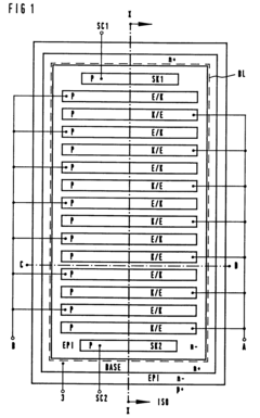
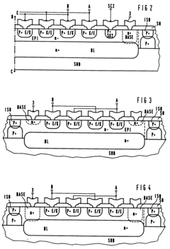
Monolithically integrated PNP transistor structure
PatentInactiveEP0570864A2
Innovation
- A monolithically integrated pnp transistor structure with symmetric emitter and collector regions, interlocking in a comb-like manner, allowing for equal current amplification in both directions with heavily doped regions and optional sense collectors to control saturation, reducing the semiconductor area requirement.
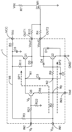
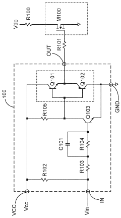
Circuit arrangement for controlling a load
PatentWO2024089263A1
Innovation
- A circuit arrangement using a PNP and NPN bipolar transistor configuration with capacitive and resistive signal paths to enhance voltage swing and reduce quiescent current, along with an enable signal input to control operation, ensuring efficient switching and preventing cross-currents.
Power Efficiency in PNP-based Designs
Power efficiency is a critical consideration in PNP-based circuit designs, particularly when aiming for compact and energy-efficient solutions. PNP transistors, when strategically implemented, can contribute significantly to reducing power consumption in various electronic applications. One of the primary advantages of PNP transistors in power-efficient designs is their ability to control current flow with minimal voltage drop, making them ideal for low-power applications.
In compact circuit designs, PNP transistors can be utilized as efficient current sources or switches, allowing for precise control of power distribution. By leveraging the inherent characteristics of PNP transistors, designers can create circuits that operate with lower supply voltages, thereby reducing overall power consumption. This is particularly beneficial in battery-powered devices where extending operational life is paramount.
The use of PNP transistors in complementary pairs with NPN transistors, known as complementary bipolar logic, offers another avenue for power efficiency. This configuration allows for push-pull output stages that minimize static power consumption, as only one transistor conducts at a time. Such arrangements are commonly found in audio amplifiers and voltage regulators, where they contribute to improved efficiency and reduced heat dissipation.
Advanced circuit topologies incorporating PNP transistors can further enhance power efficiency. For instance, current mirror configurations using PNP transistors can provide stable current sources with minimal voltage overhead, crucial for low-power analog circuits. Additionally, PNP transistors in Darlington pair arrangements can offer high current gain with relatively low power consumption, making them suitable for driving loads in compact designs where space and power are at a premium.
In the realm of power management, PNP transistors play a vital role in voltage regulation and battery charging circuits. Their ability to handle reverse current flow efficiently makes them ideal for protecting against battery discharge and implementing reverse polarity protection. Moreover, PNP transistors can be employed in low-dropout (LDO) regulators, providing stable output voltages with minimal input-output differential, thus improving overall system efficiency.
The integration of PNP transistors in modern integrated circuits (ICs) has further expanded their utility in power-efficient designs. Many ICs now incorporate PNP structures alongside other components, allowing for more sophisticated power management solutions within a single chip. This integration not only saves space but also reduces power losses associated with interconnects between discrete components.
As the demand for compact, energy-efficient electronic devices continues to grow, the role of PNP transistors in power-efficient circuit design remains crucial. Ongoing research and development in semiconductor technology are likely to yield PNP transistors with even better performance characteristics, further enhancing their applicability in low-power, compact circuit designs.
Thermal Management Strategies for Compact PNP Circuits
Thermal management is a critical aspect of compact circuit design, especially when leveraging PNP transistors. As circuit densities increase and form factors shrink, the challenge of dissipating heat becomes more pronounced. Effective thermal management strategies are essential to maintain optimal performance, reliability, and longevity of compact PNP circuits.
One primary approach to thermal management in compact PNP circuits is through careful component selection and layout optimization. Choosing PNP transistors with lower power dissipation characteristics and higher thermal resistance can significantly reduce heat generation. Additionally, strategic placement of components on the PCB, with heat-generating elements spaced apart, can help distribute thermal load more evenly.
Implementing thermal vias and copper planes is another effective strategy for managing heat in compact PNP circuits. Thermal vias, which are plated through-holes, provide a low-resistance path for heat to travel from one layer of the PCB to another. By placing these vias near PNP transistors, heat can be efficiently conducted away from the device. Copper planes, with their excellent thermal conductivity, act as heat spreaders, distributing heat across a larger surface area for more effective dissipation.
Active cooling solutions, such as miniature fans or thermoelectric coolers, can be employed in scenarios where passive cooling is insufficient. These components can be strategically integrated into the compact design to provide targeted cooling to critical areas. However, their use must be balanced against power consumption and space constraints inherent in compact circuit designs.
The application of thermal interface materials (TIMs) is crucial in enhancing heat transfer between PNP transistors and heat sinks or the PCB itself. High-performance thermal greases, phase-change materials, or thermally conductive adhesives can significantly reduce thermal resistance at component interfaces, improving overall heat dissipation efficiency.
Enclosure design plays a vital role in thermal management for compact PNP circuits. Incorporating ventilation holes, heat fins, or using thermally conductive materials for the enclosure can facilitate natural convection and improve heat dissipation. In some cases, the enclosure itself can be designed to act as a heat sink, providing an additional pathway for heat removal.
Advanced thermal simulation and modeling techniques are invaluable tools in developing effective thermal management strategies for compact PNP circuits. Computational fluid dynamics (CFD) simulations can predict heat distribution and airflow patterns, allowing designers to optimize component placement and identify potential hotspots before physical prototyping.
Implementing temperature monitoring and dynamic thermal management can further enhance the reliability of compact PNP circuits. By integrating temperature sensors and control circuits, the system can adjust its operation based on thermal conditions, potentially reducing clock speeds or shutting down non-essential components to prevent overheating.
Unlock deeper insights with Patsnap Eureka Quick Research — get a full tech report to explore trends and direct your research. Try now!
Generate Your Research Report Instantly with AI Agent
Supercharge your innovation with Patsnap Eureka AI Agent Platform!