

PNP Transistor Evolution: Higher Switching Speeds and Performance
JUL 28, 20259 MIN READ
Generate Your Research Report Instantly with AI Agent
Patsnap Eureka helps you evaluate technical feasibility & market potential.
PNP Transistor Background and Objectives
PNP transistors have played a crucial role in the evolution of electronic devices since their inception in the mid-20th century. These semiconductor devices, characterized by their ability to control current flow through the manipulation of charge carriers, have undergone significant advancements in terms of switching speeds and overall performance.
The development of PNP transistors can be traced back to the early days of semiconductor research, with the first practical bipolar junction transistor (BJT) being invented in 1947. Initially, PNP transistors were primarily used in low-frequency applications due to their limited switching capabilities. However, as technology progressed, researchers and engineers focused on improving their performance to meet the growing demands of the electronics industry.
Throughout the decades, the primary objective in PNP transistor evolution has been to achieve higher switching speeds and enhanced performance. This goal has been driven by the need for faster and more efficient electronic devices across various sectors, including telecommunications, computing, and consumer electronics. The pursuit of higher switching speeds has been particularly crucial in digital applications, where rapid on-off transitions are essential for processing information quickly and efficiently.
One of the key challenges in improving PNP transistor performance has been overcoming the inherent limitations of the device structure. Traditional PNP transistors faced issues such as slower carrier mobility compared to their NPN counterparts, which resulted in lower switching speeds. To address this, researchers have explored various techniques, including optimizing doping profiles, reducing parasitic capacitances, and implementing advanced manufacturing processes.
The evolution of PNP transistors has been closely tied to advancements in semiconductor fabrication technologies. The transition from germanium to silicon as the primary semiconductor material marked a significant milestone in transistor development. Silicon-based PNP transistors offered improved temperature stability and higher operating frequencies, paving the way for their widespread adoption in electronic circuits.
In recent years, the focus has shifted towards developing PNP transistors with nanoscale dimensions, leveraging cutting-edge fabrication techniques such as extreme ultraviolet (EUV) lithography. These advancements have enabled the creation of transistors with smaller feature sizes, leading to improved switching speeds and reduced power consumption. Additionally, the integration of novel materials and structures, such as silicon-germanium (SiGe) alloys and heterojunction bipolar transistors (HBTs), has further enhanced the performance capabilities of PNP devices.
The ongoing evolution of PNP transistors continues to be driven by the relentless pursuit of higher switching speeds and improved performance metrics. As we look towards the future, emerging technologies such as quantum computing and neuromorphic systems present new challenges and opportunities for PNP transistor development. The ultimate goal remains to push the boundaries of semiconductor technology, enabling the creation of faster, more efficient, and more powerful electronic devices that can meet the ever-increasing demands of our digital world.
Market Demand Analysis for High-Speed PNP Transistors
The market demand for high-speed PNP transistors has been steadily increasing in recent years, driven by the growing need for faster and more efficient electronic devices across various industries. As technology continues to advance, the demand for transistors with higher switching speeds and improved performance has become paramount in sectors such as telecommunications, automotive electronics, and consumer electronics.
In the telecommunications industry, the rollout of 5G networks and the ongoing development of 6G technology have created a significant demand for high-speed PNP transistors. These components are crucial in the design of advanced radio frequency (RF) amplifiers and switches, which are essential for achieving the high data rates and low latency required in modern wireless communication systems.
The automotive sector has also emerged as a major driver of demand for high-speed PNP transistors. With the increasing adoption of electric vehicles (EVs) and advanced driver assistance systems (ADAS), there is a growing need for faster and more efficient power management and control systems. High-speed PNP transistors play a vital role in these applications, enabling rapid switching in power converters and motor control circuits, thus improving overall vehicle performance and energy efficiency.
Consumer electronics represent another significant market for high-speed PNP transistors. As smartphones, tablets, and other portable devices continue to evolve, manufacturers are constantly seeking ways to improve processing speed, reduce power consumption, and enhance overall performance. High-speed PNP transistors are instrumental in achieving these goals, particularly in power management circuits and audio amplifiers.
The industrial automation sector is also contributing to the increased demand for high-speed PNP transistors. As factories become more automated and interconnected, there is a growing need for faster and more precise control systems. High-speed PNP transistors are essential components in motor drivers, sensor interfaces, and communication modules used in industrial automation applications.
Market analysts project that the global market for high-speed transistors, including PNP types, will continue to grow at a compound annual growth rate (CAGR) of over 8% in the coming years. This growth is expected to be driven by the ongoing digital transformation across industries and the increasing adoption of Internet of Things (IoT) devices, which require high-performance components for efficient operation.
However, it is important to note that the market for high-speed PNP transistors faces some challenges. The ongoing global semiconductor shortage has impacted the availability and pricing of these components, leading to supply chain disruptions and increased costs for manufacturers. Additionally, the market is highly competitive, with several major players vying for market share through continuous innovation and product development.
Current PNP Transistor Technology Challenges
PNP transistors, while essential in many electronic applications, face several significant challenges in meeting the demands of modern high-speed and high-performance circuits. One of the primary obstacles is the inherently slower switching speed compared to their NPN counterparts. This limitation stems from the fundamental physics of hole mobility in semiconductor materials, which is typically lower than electron mobility. As a result, PNP transistors struggle to achieve the rapid on-off transitions required in cutting-edge digital and analog circuits.
Another critical challenge is the difficulty in scaling PNP transistors to smaller dimensions while maintaining performance. As device sizes shrink, issues such as increased parasitic capacitance and resistance become more pronounced, further impacting switching speeds and overall efficiency. This scaling problem is particularly acute in integrated circuit designs where space is at a premium, and every nanosecond of delay can significantly affect system performance.
Power dissipation presents yet another hurdle for PNP transistor technology. As switching speeds increase, so does the power consumption, leading to thermal management issues in densely packed circuits. This challenge is exacerbated by the fact that PNP transistors often require higher operating voltages to achieve comparable performance to NPN devices, further contributing to power inefficiencies.
The manufacturing process for high-performance PNP transistors also poses significant challenges. Achieving precise doping profiles and maintaining consistent electrical characteristics across large production runs remains a complex task. This complexity often results in higher production costs and lower yields compared to NPN transistors, making PNP devices less economically viable for mass-market applications.
Furthermore, the integration of PNP transistors with other semiconductor technologies, such as CMOS, presents compatibility issues. The different processing requirements and thermal budgets can complicate fabrication processes and limit the ability to create truly optimized mixed-signal circuits.
Noise performance is another area where PNP transistors face challenges, particularly in analog and RF applications. The inherent characteristics of PNP devices often result in higher noise figures compared to NPN transistors, limiting their use in sensitive, low-noise circuits.
Lastly, the development of new materials and structures to enhance PNP transistor performance is an ongoing challenge. While innovations such as SiGe heterojunction bipolar transistors have shown promise, widespread adoption and integration of these advanced technologies into mainstream production remain limited by cost and manufacturing complexity factors.
Current High-Speed PNP Transistor Solutions
01 Circuit design for improved switching speed
Various circuit designs can be implemented to enhance the switching speed of PNP transistors. These designs may include optimized base drive circuits, feedback mechanisms, or specialized biasing techniques that reduce charge storage and minimize switching delays.- Circuit design for improved switching speed: Various circuit designs can be implemented to enhance the switching speed of PNP transistors. These designs may include optimized base-emitter junction configurations, reduced parasitic capacitances, and improved current steering techniques. Such circuit-level optimizations can significantly reduce the turn-on and turn-off times of PNP transistors, leading to faster overall switching performance.
- Semiconductor structure modifications: Modifications to the semiconductor structure of PNP transistors can lead to improved switching speeds. These modifications may include optimized doping profiles, reduced base width, and enhanced carrier mobility. By altering the physical characteristics of the transistor, the charge carrier transit time can be reduced, resulting in faster switching capabilities.
- Advanced materials and fabrication techniques: The use of advanced materials and fabrication techniques can significantly improve PNP transistor switching speed. This may involve the incorporation of novel semiconductor materials, such as silicon-germanium alloys, or the implementation of advanced fabrication processes like selective epitaxial growth. These approaches can lead to enhanced carrier mobility and reduced parasitic effects, resulting in faster switching performance.
- Biasing and operating condition optimization: Optimizing the biasing and operating conditions of PNP transistors can lead to improved switching speeds. This may include techniques such as adaptive biasing, temperature compensation, and dynamic voltage scaling. By carefully controlling the operating point of the transistor, switching delays can be minimized, and overall performance can be enhanced.
- Integration with high-speed circuit topologies: Integrating PNP transistors into high-speed circuit topologies can improve overall switching performance. This may involve the use of current-mode logic, emitter-coupled logic, or other advanced circuit configurations. By leveraging these high-speed topologies, the inherent limitations of PNP transistors can be mitigated, resulting in faster switching speeds in complex systems.
02 Semiconductor structure optimization
The physical structure of PNP transistors can be optimized to improve switching speed. This may involve modifications to the doping profiles, junction geometries, or the introduction of specialized layers to reduce parasitic capacitances and enhance carrier mobility.Expand Specific Solutions03 Use of advanced materials
Incorporating advanced materials in PNP transistor fabrication can lead to improved switching speeds. This may include the use of compound semiconductors, heterojunction structures, or novel insulating materials to enhance carrier transport and reduce parasitic effects.Expand Specific Solutions04 Integration with other components
Integrating PNP transistors with other circuit components or utilizing specialized packaging techniques can improve overall switching performance. This may involve the use of integrated circuits, hybrid designs, or advanced interconnect technologies to minimize signal propagation delays.Expand Specific Solutions05 Compensation and control techniques
Various compensation and control techniques can be employed to enhance PNP transistor switching speed. These may include temperature compensation circuits, adaptive biasing schemes, or feedback mechanisms that dynamically adjust transistor operation for optimal switching performance.Expand Specific Solutions
Key Players in PNP Transistor Industry
The PNP transistor evolution market is in a mature stage, with ongoing advancements focused on improving switching speeds and performance. The global market size for PNP transistors is substantial, driven by increasing demand in various electronic applications. Technologically, the field is well-established but continues to progress, with companies like IBM, Texas Instruments, and Infineon Technologies leading innovation. These firms, along with others such as GlobalFoundries and STMicroelectronics, are pushing the boundaries of PNP transistor capabilities, particularly in areas of high-frequency performance and power efficiency. The competitive landscape is characterized by a mix of established semiconductor giants and specialized foundries, each contributing to the ongoing evolution of PNP transistor technology.
International Business Machines Corp.
Technical Solution: IBM has made significant strides in PNP transistor evolution, focusing on enhancing switching speeds and overall performance. Their approach involves advanced silicon-germanium (SiGe) heterojunction bipolar transistors (HBTs) technology. IBM's SiGe HBTs have demonstrated cut-off frequencies exceeding 350 GHz[1], a substantial improvement over traditional silicon-based PNP transistors. The company has also developed a novel vertical PNP structure with a self-aligned emitter-base formation process, resulting in reduced parasitic capacitances and improved high-frequency performance[2]. Additionally, IBM has implemented advanced strain engineering techniques to enhance carrier mobility in the base region, further boosting switching speeds[3].
Strengths: Superior high-frequency performance, reduced parasitic capacitances, and enhanced carrier mobility. Weaknesses: Potentially higher manufacturing costs and complexity compared to traditional PNP transistors.
Texas Instruments Incorporated
Technical Solution: Texas Instruments has developed innovative solutions for PNP transistor evolution, focusing on both discrete and integrated circuit applications. Their approach includes the implementation of advanced epitaxial growth techniques to create ultra-thin base regions, resulting in significantly reduced transit times and improved switching speeds[4]. TI has also introduced a proprietary "SuperBeta" PNP transistor structure, which features a highly doped emitter and a lightly doped base, leading to current gains exceeding 1000 and improved high-frequency performance[5]. Furthermore, TI has developed advanced packaging solutions, such as chip-scale packages (CSPs) for PNP transistors, enabling better thermal management and reduced parasitic effects in high-power applications[6].
Strengths: High current gain, improved high-frequency performance, and advanced packaging solutions. Weaknesses: Potential trade-offs between high gain and voltage handling capability in some designs.
Core Innovations in PNP Transistor Technology
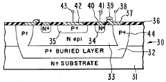
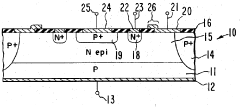
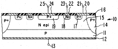
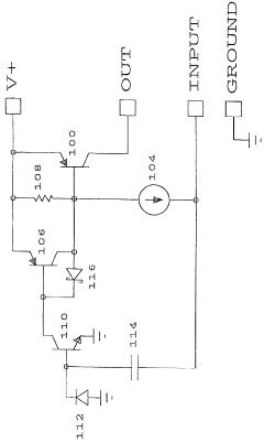
Fast switching PNP transistor
PatentInactiveUS3571674A
Innovation
- The solution involves growing an epitaxial N-type silicon layer over a P-type monocrystalline silicon substrate, diffusing a P-type emitter region into the N-type epitaxial base, and placing a metal layer over the N-type epitaxial base region to create a Schottky Barrier that parallels the base-collector junction, reducing minority carrier storage and enabling rapid switch-off times.
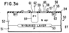
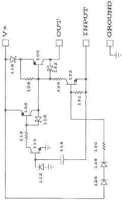
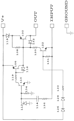
Lateral PNP fast turn-off circuit
PatentInactiveUS5903425A
Innovation
- A control circuit using a current amplifier with a PNP drive transistor and an NPN transistor, along with a capacitor and transient blocking junctions, provides a transitory reverse drive current to accelerate turn-off time and protect against high voltage transients by blocking current flow.
Material Science Advancements for PNP Transistors
Material science advancements have played a crucial role in enhancing the performance of PNP transistors, particularly in achieving higher switching speeds. The evolution of semiconductor materials has been instrumental in overcoming the inherent limitations of traditional silicon-based PNP transistors.
One of the most significant developments has been the introduction of III-V compound semiconductors, such as gallium arsenide (GaAs) and indium phosphide (InP). These materials offer superior electron mobility compared to silicon, allowing for faster charge carrier movement and, consequently, higher switching speeds. The use of GaAs in PNP transistors has enabled the creation of devices capable of operating at frequencies well into the gigahertz range.
Another breakthrough in material science has been the development of strained silicon technology. By introducing controlled strain into the silicon lattice, researchers have been able to enhance carrier mobility and improve overall transistor performance. This technique has been particularly effective in boosting the speed of PNP transistors without necessitating a complete departure from silicon-based manufacturing processes.
The exploration of two-dimensional materials, such as graphene and transition metal dichalcogenides (TMDs), has opened up new possibilities for ultra-thin, high-performance PNP transistors. These materials exhibit exceptional electrical properties and can be scaled down to atomic thicknesses, potentially leading to transistors with unprecedented switching speeds and energy efficiency.
Advancements in doping techniques have also contributed significantly to PNP transistor evolution. Precise control over dopant profiles and concentrations has allowed for the creation of optimized device structures with improved carrier transport characteristics. Techniques such as delta doping and modulation doping have enabled the fabrication of PNP transistors with enhanced performance and reduced parasitic effects.
The development of novel dielectric materials has further boosted PNP transistor capabilities. High-k dielectrics, such as hafnium oxide and zirconium oxide, have allowed for better gate control and reduced leakage currents, enabling the scaling of transistors to smaller dimensions while maintaining or improving their switching performance.
Lastly, the integration of nanomaterials, such as carbon nanotubes and semiconductor nanowires, into PNP transistor designs has shown promise in pushing the boundaries of device performance. These materials offer unique electrical and mechanical properties that can be leveraged to create transistors with exceptional switching speeds and reduced power consumption.
Environmental Impact of PNP Transistor Manufacturing
The manufacturing of PNP transistors, while crucial for technological advancement, carries significant environmental implications. The production process involves several stages that can impact the environment, including raw material extraction, fabrication, and waste management. Silicon, the primary material used in transistor manufacturing, is typically obtained through energy-intensive mining and refining processes. These activities can lead to habitat disruption, soil erosion, and water pollution in mining areas.
During the fabrication phase, the production of PNP transistors requires the use of various chemicals, including dopants, etchants, and cleaning agents. Many of these substances are toxic and can pose risks to both human health and the environment if not properly handled and disposed of. The manufacturing process also consumes substantial amounts of water, particularly for cleaning and cooling purposes, potentially straining local water resources in areas where production facilities are located.
Energy consumption is another significant environmental concern in PNP transistor manufacturing. The production of high-purity silicon and the operation of cleanroom facilities demand considerable electricity, often sourced from fossil fuels. This contributes to greenhouse gas emissions and exacerbates climate change concerns. As the demand for faster and more efficient transistors grows, the energy requirements for their production may increase, further amplifying these environmental impacts.
Waste management presents additional challenges in the transistor manufacturing industry. The production process generates various forms of waste, including chemical byproducts, contaminated water, and discarded silicon wafers. Proper treatment and disposal of these materials are essential to prevent environmental contamination and protect public health. Some manufacturers have implemented recycling programs for silicon wafers and other materials, but the overall industry still faces challenges in minimizing waste and improving resource efficiency.
As the industry evolves to produce PNP transistors with higher switching speeds and improved performance, new manufacturing techniques and materials may be introduced. While these advancements aim to enhance transistor capabilities, they may also bring unforeseen environmental consequences. For instance, the use of new dopants or novel fabrication methods could introduce additional environmental risks that require careful assessment and mitigation strategies.
To address these environmental concerns, many semiconductor manufacturers are adopting more sustainable practices. These include implementing energy-efficient production technologies, developing closed-loop water recycling systems, and exploring alternative materials with lower environmental impacts. Additionally, some companies are investing in renewable energy sources to power their facilities, reducing their carbon footprint. As the industry continues to push the boundaries of PNP transistor performance, balancing technological progress with environmental stewardship remains a critical challenge for manufacturers and policymakers alike.
Unlock deeper insights with Patsnap Eureka Quick Research — get a full tech report to explore trends and direct your research. Try now!
Generate Your Research Report Instantly with AI Agent
Supercharge your innovation with Patsnap Eureka AI Agent Platform!