How to Calculate PNP Transistor Biasing for Optimal Output?
JUL 28, 20259 MIN READ
Generate Your Research Report Instantly with AI Agent
Patsnap Eureka helps you evaluate technical feasibility & market potential.
PNP Transistor Basics and Biasing Objectives
PNP transistors are fundamental components in electronic circuits, playing a crucial role in signal amplification and switching applications. These devices operate on the principle of current flow from the emitter to the collector when a small current is applied to the base. Understanding the basics of PNP transistors is essential for effective biasing and optimal circuit performance.
The primary objective of PNP transistor biasing is to establish a stable operating point that ensures the transistor functions within its linear region. This operating point, also known as the Q-point (quiescent point), is critical for maintaining consistent amplification and preventing distortion in the output signal. Proper biasing also helps in maximizing the transistor's efficiency and extending its operational lifespan.
To achieve optimal output, the biasing process must consider several key factors. First, the collector-emitter voltage (VCE) needs to be set at an appropriate level to ensure the transistor operates in its active region. This voltage is typically maintained between the saturation and cutoff points, allowing for maximum signal swing without distortion.
Second, the base current must be carefully controlled to establish the desired collector current. The relationship between these currents, known as the current gain or beta (β), is a crucial parameter in determining the transistor's performance. By manipulating the base current, engineers can control the amplification factor and power dissipation of the circuit.
Temperature stability is another critical aspect of PNP transistor biasing. As temperature fluctuates, the transistor's characteristics can change, potentially shifting the Q-point and altering circuit performance. Implementing temperature compensation techniques, such as using resistor networks or thermistors, helps maintain stable operation across a range of environmental conditions.
The choice of biasing configuration also plays a significant role in achieving optimal output. Common biasing methods for PNP transistors include fixed bias, voltage divider bias, and emitter feedback bias. Each method offers different advantages in terms of stability, simplicity, and performance, and the selection depends on the specific requirements of the application.
Furthermore, the biasing process must account for the transistor's specifications, including its maximum collector current, power dissipation limits, and frequency response characteristics. Balancing these parameters ensures that the transistor operates efficiently without exceeding its rated limits, thus preventing damage and ensuring long-term reliability.
In conclusion, calculating PNP transistor biasing for optimal output requires a comprehensive understanding of transistor physics, circuit theory, and practical considerations. By carefully selecting the biasing method, setting appropriate voltage and current levels, and implementing necessary compensation techniques, engineers can achieve stable and efficient transistor operation, leading to improved overall circuit performance.
Market Demand for PNP Transistor Applications
The market demand for PNP transistor applications has been steadily growing, driven by the increasing complexity and miniaturization of electronic devices. PNP transistors play a crucial role in various sectors, including consumer electronics, automotive, industrial automation, and telecommunications. The global semiconductor market, which encompasses transistors, is projected to reach significant growth in the coming years, with PNP transistors contributing to this expansion.
In the consumer electronics sector, PNP transistors are extensively used in smartphones, tablets, and wearable devices. The demand for these devices continues to rise, particularly in emerging markets, fueling the need for PNP transistors in power management circuits, audio amplifiers, and signal processing applications. The automotive industry also presents a substantial market for PNP transistors, as modern vehicles incorporate more electronic systems for safety, infotainment, and powertrain control.
The industrial automation sector is another key driver of PNP transistor demand. As factories and manufacturing processes become increasingly digitized and automated, the need for precise control and sensing components grows. PNP transistors are essential in industrial control systems, robotics, and sensor interfaces, contributing to the overall efficiency and productivity of manufacturing operations.
Telecommunications infrastructure, including 5G networks, relies heavily on PNP transistors for signal amplification and switching applications. The ongoing global rollout of 5G technology is expected to sustain strong demand for PNP transistors in the coming years. Additionally, the Internet of Things (IoT) ecosystem, which encompasses a wide range of connected devices and sensors, presents a significant growth opportunity for PNP transistor applications.
The medical electronics sector is emerging as a promising market for PNP transistors. Advanced medical devices, such as portable diagnostic equipment and implantable devices, require high-performance, low-power transistors for their operation. As healthcare systems worldwide focus on improving patient care and adopting telemedicine solutions, the demand for PNP transistors in medical applications is expected to increase.
Energy efficiency and power management considerations are driving innovation in PNP transistor design and applications. With the growing emphasis on reducing power consumption in electronic devices, manufacturers are seeking transistors with improved performance characteristics and lower power requirements. This trend is likely to stimulate research and development efforts in PNP transistor technology, potentially leading to new market opportunities.
As the demand for PNP transistors continues to grow across various industries, manufacturers are focusing on developing advanced fabrication techniques and materials to enhance transistor performance and reduce costs. The market is also witnessing a shift towards specialized PNP transistors designed for specific applications, such as high-frequency operations or extreme temperature environments, catering to niche market segments with unique requirements.
Current Challenges in PNP Transistor Biasing
Despite significant advancements in transistor technology, PNP transistor biasing for optimal output remains a challenging aspect of circuit design. One of the primary difficulties lies in achieving precise control over the base current, which directly impacts the collector current and overall transistor performance. The sensitivity of PNP transistors to temperature variations further complicates the biasing process, as thermal effects can lead to unstable operating points and reduced reliability.
Another major challenge is the inherent lower mobility of holes compared to electrons, which results in PNP transistors having lower current gain and frequency response than their NPN counterparts. This characteristic makes it more difficult to achieve high-frequency performance and requires careful consideration when designing circuits for applications that demand rapid switching or high-speed operation.
The issue of Early effect, which causes the collector current to increase with increasing collector-emitter voltage, poses additional complications in PNP transistor biasing. This effect can lead to non-linear behavior and reduced output resistance, making it challenging to maintain consistent performance across different operating conditions.
Furthermore, the selection of appropriate biasing resistors presents a significant challenge. Designers must strike a delicate balance between ensuring stable operation and minimizing power consumption. Too high resistance values may lead to insufficient base current, while too low values can result in excessive power dissipation and reduced efficiency.
The parasitic capacitances inherent in PNP transistors, particularly the base-emitter and collector-base capacitances, introduce frequency-dependent effects that can impact circuit performance. These capacitances can limit the high-frequency response and cause unwanted oscillations if not properly accounted for in the biasing design.
Another challenge in PNP transistor biasing is addressing the issue of reverse saturation current, which can lead to undesired leakage currents and affect the overall circuit performance. This becomes particularly critical in low-power applications where minimizing standby current is essential.
Lastly, the variability in transistor parameters due to manufacturing tolerances and process variations adds another layer of complexity to the biasing process. Designers must account for these variations to ensure robust circuit operation across a range of transistor characteristics, often necessitating the use of feedback mechanisms or compensation techniques to maintain optimal performance.
Existing PNP Biasing Calculation Methods
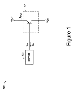
01 PNP transistor output circuit design
PNP transistor output circuits are designed to provide efficient current sourcing capabilities. These circuits often include biasing networks, feedback mechanisms, and protection elements to ensure stable operation and optimal performance. The design considerations include voltage levels, current requirements, and temperature compensation.- PNP transistor output circuit design: PNP transistor output circuits are designed to provide specific electrical characteristics and performance. These circuits often include components such as resistors and capacitors to control current flow, voltage levels, and switching behavior. The design focuses on optimizing factors like gain, bandwidth, and power efficiency for various applications.
- PNP transistor in power management applications: PNP transistors are utilized in power management circuits to regulate voltage and current. These applications often involve the transistor acting as a switch or amplifier to control power distribution, protect against overcurrent conditions, or manage battery charging processes. The PNP configuration allows for efficient high-side switching in many power control scenarios.
- Integration of PNP transistors in semiconductor devices: PNP transistors are integrated into various semiconductor devices and integrated circuits. This integration involves specific fabrication techniques to create the P-type and N-type regions within the silicon substrate. The process may include steps such as ion implantation, diffusion, and epitaxial growth to achieve the desired transistor characteristics and performance.
- PNP transistor output in analog circuit applications: PNP transistors are employed in analog circuits for applications such as amplifiers, current mirrors, and voltage references. The output characteristics of PNP transistors in these circuits are crucial for maintaining signal integrity, achieving high linearity, and ensuring stable performance across varying operating conditions. Careful biasing and load selection are essential for optimal analog circuit operation.
- Temperature compensation in PNP transistor outputs: Temperature compensation techniques are applied to PNP transistor outputs to maintain consistent performance across varying thermal conditions. These methods may involve the use of complementary NPN transistors, thermistors, or other temperature-sensitive components to adjust bias voltages or currents. The goal is to minimize the impact of temperature variations on the transistor's output characteristics and overall circuit behavior.
02 Integration of PNP transistors in semiconductor devices
PNP transistors are integrated into various semiconductor devices, including integrated circuits and power management systems. The integration process involves careful consideration of device layout, doping profiles, and isolation techniques to achieve desired electrical characteristics and minimize parasitic effects.Expand Specific Solutions03 PNP transistor output for power applications
PNP transistors are utilized in power applications to provide high-current output capabilities. These applications often require careful thermal management, current limiting features, and protection against overcurrent and overvoltage conditions. The design focuses on maximizing efficiency and reliability in power delivery.Expand Specific Solutions04 PNP transistor output in analog circuits
PNP transistors are employed in various analog circuit configurations, such as current mirrors, voltage regulators, and amplifiers. The output characteristics of PNP transistors are leveraged to achieve precise current control, voltage referencing, and signal amplification in these applications.Expand Specific Solutions05 PNP transistor output for logic and switching applications
PNP transistors are used in logic circuits and switching applications to provide high-side switching capabilities and level shifting functions. These designs often incorporate techniques to minimize switching losses, reduce propagation delays, and ensure compatibility with various logic families.Expand Specific Solutions
Key Players in Semiconductor Industry
The competition landscape for PNP transistor biasing optimization is in a mature phase, with a well-established market and significant technological advancements. Major players like Texas Instruments, Qualcomm, and NXP Semiconductors dominate the field, leveraging their extensive R&D capabilities and industry experience. The market size is substantial, driven by the widespread use of transistors in various electronic applications. Technological maturity is high, with companies like Infineon Technologies and STMicroelectronics continuously refining biasing techniques for improved performance and efficiency. However, emerging players and research institutions are exploring novel approaches, potentially disrupting the current market dynamics.
Texas Instruments Incorporated
Technical Solution: Texas Instruments (TI) has developed advanced PNP transistor biasing techniques for optimal output. Their approach involves using precision voltage references and temperature-compensated current sources to ensure stable biasing across varying conditions. TI's solution incorporates integrated bias circuits that automatically adjust for temperature and supply voltage variations, maintaining consistent performance[1]. They have also implemented adaptive biasing techniques that optimize power consumption based on the required output performance, significantly improving overall efficiency[3]. TI's PNP transistor biasing solutions often include on-chip trimming capabilities to fine-tune bias points during manufacturing, ensuring tight tolerances and improved yield[5].
Strengths: Highly integrated solutions, excellent temperature stability, and adaptive power optimization. Weaknesses: Potentially higher cost for fully integrated solutions and may require specialized design knowledge to implement effectively.
QUALCOMM, Inc.
Technical Solution: Qualcomm has innovated in PNP transistor biasing for optimal output, particularly in the context of RF power amplifiers and low-noise amplifiers used in mobile communications. Their approach focuses on dynamic biasing techniques that adjust the transistor operating point based on the input signal level and desired output power[2]. Qualcomm's solutions often incorporate envelope tracking systems that modulate the bias voltage in real-time to maintain high efficiency across a wide range of output powers[4]. They have also developed advanced thermal management techniques integrated into their biasing circuits to prevent performance degradation under high-power conditions[6]. Qualcomm's PNP transistor biasing methods typically include digitally controlled bias networks that allow for software-based optimization and calibration in the field[8].
Strengths: Highly efficient for RF applications, excellent dynamic range, and software-configurable bias points. Weaknesses: Complexity in implementation and potential for increased power consumption in control circuitry.
Core Innovations in Transistor Biasing
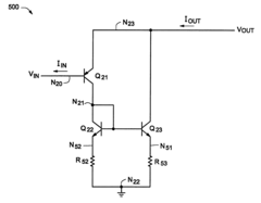
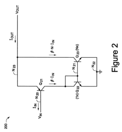
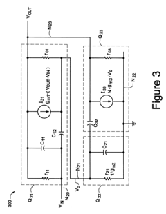
PNP multiplier
PatentInactiveUS6614284B1
Innovation
- A PNP multiplier circuit employing a small PNP transistor coupled with a current mirror, where the current mirror scales the collector current by a factor of N, effectively increasing the current gain to β.(N+1), allowing for comparable performance to a large PNP transistor without the need for large die area.
Direct-coupled PNP transistor pull-up ECL circuits and direct-coupled complementary push-pull ECL circuits
PatentInactiveUS5334886A
Innovation
- A direct-coupled PNP transistor pull-up scheme is introduced, where the PNP transistor is biased by direct tapping of existing voltage levels in the ECL circuit, eliminating the need for extra biasing circuits and utilizing dynamic current to pull up the output node when the input signal goes to a logical low level.
Temperature Effects on PNP Biasing
Temperature plays a crucial role in the performance and reliability of PNP transistor biasing circuits. As ambient temperature fluctuates, it can significantly impact the transistor's characteristics, leading to changes in collector current, base-emitter voltage, and overall circuit behavior. Understanding these temperature effects is essential for designing robust and stable PNP biasing configurations.
One of the primary temperature-dependent parameters in PNP transistors is the base-emitter voltage (VBE). As temperature increases, VBE decreases at a rate of approximately -2mV/°C. This inverse relationship can lead to thermal runaway if not properly compensated. The collector current (IC) is also affected by temperature changes, typically increasing with rising temperatures due to the reduction in VBE.
The current gain (β or hFE) of PNP transistors is another parameter sensitive to temperature variations. Generally, β increases with temperature, which can result in amplified collector current changes and potential instability in the biasing circuit. This effect is particularly pronounced in high-power applications where significant heat dissipation occurs.
To mitigate temperature-induced variations in PNP biasing, several compensation techniques can be employed. One common approach is the use of negative feedback in the biasing network. By incorporating resistors in the emitter and collector paths, the circuit can self-adjust to maintain a more stable operating point across temperature fluctuations.
Thermistors or temperature-sensitive resistors can be integrated into the biasing network to provide active temperature compensation. These components change their resistance in response to temperature variations, helping to counteract the effects on transistor parameters and maintain consistent biasing conditions.
Another effective method for temperature stabilization is the implementation of a constant-current source in the biasing circuit. This approach helps maintain a steady collector current regardless of temperature-induced changes in transistor characteristics. Voltage reference circuits, such as bandgap references, can also be utilized to provide temperature-independent bias voltages.
In high-precision applications, more advanced techniques like on-chip temperature sensing and digital compensation may be employed. These methods involve real-time monitoring of the transistor's temperature and dynamic adjustment of biasing parameters to ensure optimal performance across a wide temperature range.
When designing PNP biasing circuits for extreme temperature environments, special considerations must be made. Selection of components with appropriate temperature coefficients and the use of temperature-resistant materials become critical. Additionally, thermal management techniques, such as heat sinking and proper PCB layout, play a vital role in maintaining stable operating conditions.
Simulation Tools for Transistor Biasing
Simulation tools play a crucial role in the design and optimization of PNP transistor biasing circuits. These tools provide engineers with the ability to model, analyze, and predict the behavior of transistor circuits before physical implementation. One of the most widely used simulation tools in the industry is SPICE (Simulation Program with Integrated Circuit Emphasis), which offers a comprehensive platform for transistor biasing analysis.
SPICE simulators, such as LTspice, PSpice, and Ngspice, allow designers to create virtual circuit models and perform various types of analyses, including DC operating point, AC small-signal, and transient simulations. These tools enable engineers to accurately calculate and optimize PNP transistor biasing parameters, such as collector current, base-emitter voltage, and collector-emitter voltage, under different operating conditions.
Advanced simulation tools often incorporate sophisticated transistor models that account for various physical phenomena, including temperature effects, parasitic capacitances, and high-frequency behavior. These models enhance the accuracy of biasing calculations and help predict the transistor's performance across a wide range of operating conditions.
Many simulation tools also offer built-in optimization algorithms that can automatically adjust circuit parameters to achieve desired performance metrics. This feature is particularly useful when designing PNP transistor biasing circuits for specific applications, as it can significantly reduce the time and effort required to achieve optimal output characteristics.
In addition to traditional circuit simulators, there are specialized tools focused on transistor characterization and modeling. These tools, such as IC-CAP (Integrated Circuit Characterization and Analysis Program), allow engineers to extract accurate transistor models from measured data, which can then be used in circuit simulations for more precise biasing calculations.
Modern simulation tools often include graphical user interfaces that simplify the process of schematic entry and results visualization. These interfaces make it easier for engineers to experiment with different biasing configurations and quickly analyze the impact of parameter variations on circuit performance.
Furthermore, many simulation tools now offer cloud-based solutions, enabling collaborative design and providing access to powerful computing resources for complex circuit analyses. This trend is particularly beneficial for teams working on large-scale projects involving multiple PNP transistor stages or intricate biasing networks.
As transistor technologies continue to evolve, simulation tools are constantly updated to incorporate new device models and analysis techniques. This ongoing development ensures that engineers have access to the most accurate and efficient tools for calculating PNP transistor biasing, ultimately leading to improved circuit designs and optimal output performance.
Unlock deeper insights with Patsnap Eureka Quick Research — get a full tech report to explore trends and direct your research. Try now!
Generate Your Research Report Instantly with AI Agent
Supercharge your innovation with Patsnap Eureka AI Agent Platform!