How to Optimize PNP Transistor for Low Power Consumption?
JUL 28, 20259 MIN READ
Generate Your Research Report Instantly with AI Agent
Patsnap Eureka helps you evaluate technical feasibility & market potential.
PNP Transistor Optimization Background and Objectives
PNP transistors have been a fundamental component in electronic circuits since their inception in the mid-20th century. These devices, along with their NPN counterparts, form the backbone of bipolar junction transistor (BJT) technology. Over the years, the focus on power efficiency has become increasingly critical in electronic design, particularly with the proliferation of portable and battery-powered devices.
The evolution of PNP transistor technology has been driven by the constant demand for improved performance and reduced power consumption. Early PNP transistors were relatively inefficient and prone to high power losses, limiting their application in low-power circuits. However, advancements in semiconductor manufacturing processes and materials science have led to significant improvements in PNP transistor characteristics.
The primary objective in optimizing PNP transistors for low power consumption is to minimize energy losses while maintaining or enhancing their switching and amplification capabilities. This involves addressing several key areas, including reducing leakage currents, improving thermal management, and enhancing the overall efficiency of the device.
One of the main challenges in PNP transistor optimization has been the inherent limitations of the P-type semiconductor material. Historically, PNP transistors have been less efficient than their NPN counterparts due to the lower mobility of holes compared to electrons. This has led to ongoing research and development efforts focused on improving the characteristics of P-type materials and exploring novel semiconductor compounds.
The trend towards miniaturization in electronics has also played a crucial role in PNP transistor optimization. As device sizes shrink, new challenges emerge, such as increased susceptibility to quantum effects and heightened sensitivity to manufacturing variations. These factors necessitate innovative approaches to transistor design and fabrication to maintain performance while reducing power consumption.
Recent technological advancements have opened up new possibilities for PNP transistor optimization. The integration of advanced materials, such as silicon-germanium alloys and III-V semiconductors, has shown promise in enhancing the performance of PNP devices. Additionally, the development of novel transistor architectures, including vertical and lateral designs, has provided new avenues for improving power efficiency.
The optimization of PNP transistors for low power consumption is not only a technical challenge but also an economic imperative. As energy costs rise and environmental concerns grow, the demand for more power-efficient electronic devices continues to increase. This has led to a convergence of interests between semiconductor manufacturers, device designers, and end-users, all seeking solutions that can deliver enhanced performance with reduced power requirements.
Market Demand for Low Power Electronics
The demand for low power electronics has been steadily increasing across various sectors, driven by the growing need for energy-efficient devices and systems. This trend is particularly evident in portable consumer electronics, Internet of Things (IoT) devices, and industrial applications where power consumption is a critical factor.
In the consumer electronics market, smartphones, tablets, and wearable devices are at the forefront of low power demand. Users expect longer battery life without compromising performance, pushing manufacturers to optimize every component, including transistors. The global smartphone market, a key driver for low power electronics, continues to grow, with over 1.3 billion units shipped annually.
The IoT sector is another significant contributor to the demand for low power electronics. As the number of connected devices proliferates, reaching billions worldwide, the need for energy-efficient components becomes paramount. IoT devices often operate in remote or hard-to-reach locations, making battery life a crucial factor. This has led to increased interest in ultra-low power transistors and microcontrollers.
Industrial and automotive sectors are also embracing low power electronics. In industrial automation, wireless sensors and actuators require minimal power consumption to operate effectively over extended periods. The automotive industry, particularly with the rise of electric vehicles, demands highly efficient power management systems to maximize range and performance.
The medical device industry is another area where low power electronics are gaining traction. Implantable devices, wearable health monitors, and portable diagnostic equipment all benefit from reduced power consumption, enhancing patient comfort and device longevity.
Environmental concerns and energy regulations are further driving the demand for low power electronics. Governments worldwide are implementing stricter energy efficiency standards, encouraging manufacturers to develop more power-efficient products. This regulatory push, combined with consumer awareness of energy conservation, is creating a favorable market environment for low power electronic components.
The market for low power electronics is not limited to hardware alone. There is a growing demand for software solutions that optimize power consumption at the system level. This includes power management algorithms, sleep mode optimizations, and intelligent power distribution techniques.
As the demand for low power electronics continues to grow, the focus on optimizing components like PNP transistors becomes increasingly important. Manufacturers and researchers are investing heavily in developing new materials, designs, and fabrication techniques to push the boundaries of power efficiency. This ongoing innovation is expected to open up new applications and markets for low power electronics in the coming years.
Current PNP Transistor Technology and Challenges
PNP transistors have been a cornerstone of electronic design for decades, playing a crucial role in various applications. However, as the demand for low-power consumption devices continues to grow, optimizing PNP transistors for reduced power usage has become a significant challenge. The current state of PNP transistor technology presents both opportunities and obstacles in achieving this goal.
One of the primary challenges in optimizing PNP transistors for low power consumption lies in their inherent characteristics. PNP transistors typically have lower carrier mobility compared to their NPN counterparts, resulting in slower switching speeds and higher power dissipation. This limitation has led to a preference for NPN transistors in many high-speed, low-power applications, creating a need for innovative solutions to improve PNP performance.
Recent advancements in semiconductor manufacturing processes have yielded some improvements in PNP transistor efficiency. The introduction of advanced materials and fabrication techniques, such as silicon-germanium (SiGe) alloys and high-k dielectrics, has allowed for better control of carrier transport and reduced leakage currents. However, these improvements have not fully bridged the gap between PNP and NPN transistor performance in low-power scenarios.
Another significant challenge is the trade-off between power consumption and other critical parameters, such as gain, bandwidth, and noise performance. As designers strive to reduce power consumption, they often encounter limitations in maintaining acceptable levels of these other crucial characteristics. This balancing act requires careful optimization of transistor geometry, doping profiles, and biasing conditions.
The miniaturization of transistors, while beneficial for overall circuit density and performance, presents additional challenges for PNP optimization. As device dimensions shrink, short-channel effects become more pronounced, leading to increased leakage currents and reduced voltage gain. These effects are particularly problematic for PNP transistors, which already struggle with lower gain compared to their NPN counterparts.
Temperature sensitivity is another area of concern in PNP transistor optimization. The performance of PNP transistors can vary significantly with temperature changes, affecting their reliability and consistency in low-power applications. Developing temperature compensation techniques and improving thermal management strategies are essential aspects of current research efforts.
The integration of PNP transistors into complex analog and mixed-signal circuits poses additional challenges. Parasitic capacitances and resistances associated with PNP structures can impact overall circuit performance and power efficiency. Designers must carefully consider layout techniques and circuit topologies to minimize these parasitic effects and optimize power consumption at the system level.
Despite these challenges, ongoing research and development efforts are yielding promising results. Advanced simulation tools and modeling techniques are enabling more accurate prediction of PNP transistor behavior, allowing for better optimization strategies. Additionally, novel device structures, such as vertical PNP transistors and silicon-on-insulator (SOI) technologies, are showing potential for improved low-power performance.
Existing Low Power PNP Transistor Solutions
01 Power consumption reduction techniques in PNP transistors
Various methods are employed to reduce power consumption in PNP transistors, including optimizing circuit design, implementing power-saving modes, and utilizing advanced manufacturing processes. These techniques aim to improve energy efficiency while maintaining performance in electronic devices.- Power consumption reduction in PNP transistors: Various techniques are employed to reduce power consumption in PNP transistors, including optimizing the transistor structure, improving the base-emitter junction, and implementing advanced biasing methods. These approaches aim to minimize leakage currents and enhance overall efficiency in electronic circuits.
- Thermal management for PNP transistors: Effective thermal management strategies are crucial for controlling power consumption in PNP transistors. This includes the use of heat sinks, improved packaging designs, and thermal-aware circuit layouts to dissipate heat efficiently and maintain optimal operating temperatures.
- Power-efficient PNP transistor configurations: Innovative circuit configurations and topologies are developed to maximize the power efficiency of PNP transistors. These designs focus on optimizing current flow, reducing parasitic capacitances, and implementing advanced switching techniques to minimize power losses.
- Dynamic power management for PNP transistors: Implementing dynamic power management techniques allows for real-time adjustment of PNP transistor operation based on performance requirements. This includes adaptive biasing, power gating, and voltage scaling methods to optimize power consumption under varying load conditions.
- Integration of PNP transistors in low-power systems: Designing PNP transistors for integration into low-power systems involves considering factors such as substrate isolation, parasitic effects, and overall system architecture. This approach aims to minimize power consumption at both the transistor and system levels, ensuring optimal performance in energy-constrained applications.
02 Thermal management for PNP transistors
Effective thermal management strategies are crucial for controlling power consumption in PNP transistors. This includes heat dissipation techniques, temperature monitoring, and thermal-aware circuit design to prevent overheating and maintain optimal performance.Expand Specific Solutions03 Power-efficient PNP transistor configurations
Specific configurations and arrangements of PNP transistors are designed to minimize power consumption. These may include optimized biasing schemes, cascaded structures, and innovative circuit topologies that reduce current leakage and improve overall efficiency.Expand Specific Solutions04 Dynamic power management in PNP transistor circuits
Implementation of dynamic power management techniques allows for real-time adjustment of PNP transistor operation based on performance requirements. This includes adaptive voltage scaling, frequency modulation, and selective activation of transistor components to optimize power consumption.Expand Specific Solutions05 Integration of PNP transistors in low-power systems
PNP transistors are integrated into low-power system designs, considering factors such as supply voltage optimization, standby current reduction, and efficient power distribution. This approach ensures minimal power consumption in complex electronic systems and devices.Expand Specific Solutions
Key Players in Semiconductor Industry
The optimization of PNP transistors for low power consumption is a mature technology in a well-established market. The industry is in a mature phase, with a global market size estimated in billions of dollars. Major players like Texas Instruments, Infineon Technologies, and STMicroelectronics have significant market shares and advanced R&D capabilities. These companies, along with others such as NXP Semiconductors and ON Semiconductor, have developed sophisticated techniques for reducing power consumption in PNP transistors, including advanced process technologies and innovative circuit designs. The competition is intense, with companies continuously striving to improve efficiency and performance to maintain their market positions.
International Business Machines Corp.
Technical Solution: IBM has developed advanced PNP transistor optimization techniques for low power consumption. They utilize a combination of silicon-on-insulator (SOI) technology and strained silicon to enhance carrier mobility and reduce leakage current[1]. IBM's approach involves carefully engineered doping profiles and ultra-thin body structures to minimize parasitic capacitances. They have also implemented advanced gate stack materials and high-k dielectrics to improve electrostatic control and reduce gate leakage[2]. Furthermore, IBM has pioneered the use of SiGe in the base region of PNP transistors, which allows for band engineering and improved current gain at lower power levels[3].
Strengths: Industry-leading SOI technology, expertise in advanced materials integration, and strong research capabilities. Weaknesses: Higher manufacturing costs and complexity compared to traditional bulk CMOS processes.
Texas Instruments Incorporated
Technical Solution: Texas Instruments has focused on optimizing PNP transistors for low power applications through several innovative approaches. They have developed a proprietary BiCMOS process that integrates high-performance PNP transistors with low-power CMOS circuitry[4]. TI's optimization strategy includes the use of selective epitaxial growth for the base region, which allows for precise control of the doping profile and reduces base resistance. They have also implemented advanced isolation techniques, such as deep trench isolation, to minimize parasitic capacitances and improve high-frequency performance while maintaining low power consumption[5]. Additionally, TI has developed specialized circuit design techniques, such as current-mode logic and sub-threshold operation, to leverage their optimized PNP transistors in ultra-low-power applications[6].
Strengths: Extensive experience in analog and mixed-signal design, strong manufacturing capabilities, and a wide range of applications. Weaknesses: Potentially higher cost for specialized BiCMOS processes compared to standard CMOS.
Core Innovations in PNP Transistor Optimization
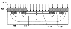
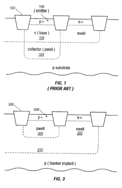
One mask PNP (or NPN) transistor allowing high performance
PatentInactiveUS6797577B2
Innovation
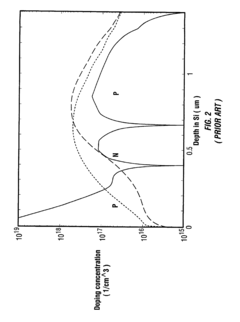
- A method is developed to form high-performance bipolar junction transistors by optimizing the collector region using a single additional mask, allowing for customized dopant concentrations and profiles, similar to the base formation, thereby enhancing performance while minimizing additional masking operations and costs.
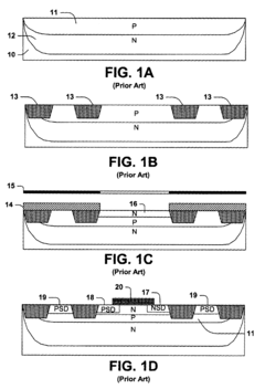
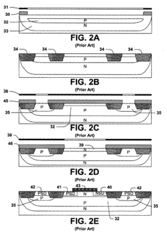
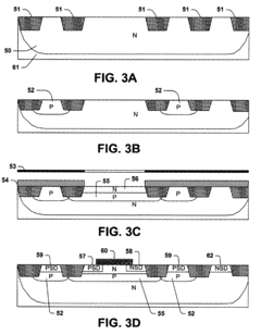
High performance PNP bipolar device fully compatible with CMOS process
PatentInactiveUS6794730B2
Innovation
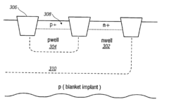
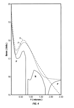
- The emitter efficiency of a vertical pnp bipolar junction transistor is improved by reducing the depth of the p well implant, increasing dopant concentration in the emitter region, and decreasing dopant concentration in the base, while using a high energy blanket boron implant for n well to n well isolation, all within the standard CMOS process without additional mask steps.
Thermal Management Strategies
Thermal management is a critical aspect of optimizing PNP transistors for low power consumption. As transistors operate, they generate heat, which can significantly impact their performance and efficiency. Effective thermal management strategies are essential to maintain optimal operating temperatures, reduce power losses, and extend the lifespan of PNP transistors in low-power applications.
One of the primary thermal management strategies for PNP transistors is the implementation of heat sinks. These passive cooling devices increase the surface area available for heat dissipation, allowing for more efficient transfer of thermal energy from the transistor to the surrounding environment. The design and material selection of heat sinks play a crucial role in their effectiveness. Aluminum and copper are commonly used materials due to their high thermal conductivity.
Active cooling methods, such as forced-air cooling or liquid cooling systems, can be employed for more demanding applications. These techniques involve the use of fans or pumps to circulate air or coolant around the transistor, enhancing heat removal. While active cooling can be highly effective, it must be carefully balanced against power consumption requirements in low-power designs.
Thermal interface materials (TIMs) are another important component of thermal management strategies. These materials, such as thermal greases, pads, or adhesives, are used to fill microscopic air gaps between the transistor and the heat sink, improving thermal conductivity and reducing thermal resistance. The selection of appropriate TIMs can significantly enhance overall cooling efficiency.
Layout and packaging considerations also play a vital role in thermal management. Proper spacing between components, strategic placement of heat-generating elements, and the use of thermally conductive packaging materials can help distribute heat more evenly and prevent localized hot spots. Additionally, the implementation of thermal vias in printed circuit boards can facilitate heat transfer from the transistor to other layers or dedicated heat-spreading planes.
Advanced thermal management techniques include the use of phase-change materials (PCMs) and thermoelectric coolers. PCMs absorb and release thermal energy during phase transitions, helping to stabilize temperatures during periods of varying heat generation. Thermoelectric coolers, based on the Peltier effect, can actively pump heat away from the transistor, providing precise temperature control in critical applications.
Simulation and modeling tools are invaluable for optimizing thermal management strategies. Computational fluid dynamics (CFD) and finite element analysis (FEA) software enable designers to predict thermal behavior, identify potential hot spots, and evaluate the effectiveness of various cooling solutions before physical prototyping. These tools can significantly reduce development time and costs while improving the overall thermal performance of PNP transistor designs.
Environmental Impact of Low Power Transistors
The optimization of PNP transistors for low power consumption has significant environmental implications, extending beyond mere energy efficiency. As electronic devices become increasingly ubiquitous, the cumulative impact of their power consumption on global energy demand and associated carbon emissions cannot be overstated. Low power transistors, including optimized PNP variants, play a crucial role in mitigating these environmental concerns.
Reduced power consumption in transistors directly translates to lower energy requirements for electronic devices. This decrease in energy demand has a cascading effect on the entire power generation and distribution chain. Power plants, whether fossil fuel-based or renewable, can operate at lower capacities, leading to reduced greenhouse gas emissions and a smaller carbon footprint for the technology sector as a whole.
The environmental benefits of low power transistors are particularly pronounced in battery-powered devices. By extending battery life, these optimized transistors reduce the frequency of battery replacements and recharging cycles. This, in turn, diminishes the environmental impact associated with battery production, disposal, and recycling processes. The reduced demand for batteries also alleviates pressure on finite resources used in their manufacture, such as lithium and cobalt.
In data centers and large-scale computing facilities, the implementation of low power transistors can result in substantial energy savings. These facilities are known for their enormous power consumption and cooling requirements. By incorporating more efficient transistors, including optimized PNP designs, the overall energy demand of these facilities can be significantly reduced. This not only lowers operational costs but also decreases the environmental footprint of the digital infrastructure that powers our increasingly connected world.
The environmental impact of low power transistors extends to electronic waste management. As devices become more energy-efficient, their lifespan tends to increase, reducing the rate at which electronic products are discarded. This slowdown in e-waste generation helps mitigate the environmental challenges associated with electronic disposal and recycling, including soil and water pollution from improperly handled hazardous materials.
Moreover, the shift towards low power transistors aligns with global initiatives for sustainable development and climate change mitigation. By enabling the creation of more energy-efficient electronic products, these transistors contribute to meeting international energy efficiency standards and environmental regulations. This technological advancement supports broader efforts to reduce global energy consumption and transition towards a more sustainable, low-carbon economy.
Unlock deeper insights with Patsnap Eureka Quick Research — get a full tech report to explore trends and direct your research. Try now!
Generate Your Research Report Instantly with AI Agent
Supercharge your innovation with Patsnap Eureka AI Agent Platform!