

How to Integrate PNP Transistors into Existing Tech Frameworks?
JUL 28, 20259 MIN READ
Generate Your Research Report Instantly with AI Agent
PatSnap Eureka helps you evaluate technical feasibility & market potential.
PNP Transistor Integration Background and Objectives
PNP transistors have been a fundamental component in electronic circuits since their invention in the mid-20th century. These devices, complementary to NPN transistors, play a crucial role in amplifying and switching electronic signals. The integration of PNP transistors into existing technological frameworks represents a significant challenge and opportunity in the field of electronics and semiconductor technology.
The evolution of PNP transistor technology has been closely tied to the broader development of semiconductor devices. From early germanium-based transistors to modern silicon and compound semiconductor implementations, PNP transistors have undergone continuous refinement in terms of performance, size, and manufacturing processes. This progression has been driven by the ever-increasing demands of electronic systems for higher speed, lower power consumption, and greater integration density.
The primary objective of integrating PNP transistors into existing tech frameworks is to enhance the functionality, efficiency, and versatility of electronic circuits and systems. This integration aims to leverage the unique characteristics of PNP transistors, such as their ability to handle positive voltage swings and their complementary behavior to NPN transistors, to create more sophisticated and optimized circuit designs.
One of the key goals is to achieve seamless integration of PNP transistors with existing CMOS (Complementary Metal-Oxide-Semiconductor) technology, which dominates modern integrated circuit design. This integration would enable the creation of more complex analog and mixed-signal circuits, potentially leading to improved performance in areas such as power management, signal processing, and sensor interfaces.
Another important objective is to address the challenges associated with PNP transistor integration, including issues related to fabrication processes, thermal management, and parasitic effects. Overcoming these challenges is crucial for realizing the full potential of PNP transistors in advanced electronic systems.
The integration effort also aims to explore new applications and design paradigms that can benefit from the unique properties of PNP transistors. This includes investigating novel circuit topologies, developing new design methodologies, and identifying emerging application areas where PNP transistors can provide significant advantages.
Furthermore, the integration of PNP transistors into existing tech frameworks is expected to contribute to the ongoing miniaturization and performance enhancement of electronic devices. By enabling more efficient and compact circuit designs, this integration could support the development of next-generation technologies in fields such as mobile communications, Internet of Things (IoT) devices, and wearable electronics.
Market Demand Analysis for PNP Transistor Integration
The integration of PNP transistors into existing technological frameworks has become increasingly crucial in the semiconductor industry, driven by the growing demand for more efficient and versatile electronic devices. Market analysis reveals a significant uptick in the adoption of PNP transistors across various sectors, particularly in power management, analog circuits, and high-frequency applications.
The global market for PNP transistors is experiencing steady growth, with a projected compound annual growth rate (CAGR) of 5.8% from 2021 to 2026. This growth is primarily fueled by the expanding consumer electronics sector, automotive industry advancements, and the proliferation of Internet of Things (IoT) devices. The automotive sector, in particular, has emerged as a key driver for PNP transistor integration, as vehicle manufacturers increasingly incorporate advanced driver assistance systems (ADAS) and electric powertrains.
In the consumer electronics segment, the demand for PNP transistors is being propelled by the need for improved power efficiency and miniaturization in smartphones, tablets, and wearable devices. The integration of PNP transistors into these devices enables better power management, longer battery life, and enhanced overall performance. This trend is expected to continue as consumers demand more feature-rich and energy-efficient electronic products.
The industrial automation sector is another significant market for PNP transistor integration. As factories and manufacturing processes become increasingly digitized and automated, the need for reliable and efficient transistor technology has grown. PNP transistors play a crucial role in sensor systems, control circuits, and power distribution networks within industrial environments.
Geographically, Asia-Pacific dominates the market for PNP transistor integration, accounting for over 40% of the global market share. This is largely due to the presence of major semiconductor manufacturers and electronic device producers in countries like China, South Korea, and Taiwan. North America and Europe follow, with strong demand driven by technological advancements in telecommunications, healthcare, and aerospace industries.
The market demand for PNP transistor integration is also influenced by emerging technologies such as 5G networks, artificial intelligence, and edge computing. These technologies require advanced semiconductor solutions that can handle higher frequencies, lower power consumption, and increased reliability. PNP transistors, when effectively integrated into existing frameworks, can address these requirements and enable the development of more sophisticated electronic systems.
However, the market faces challenges such as the ongoing global semiconductor shortage and increasing complexity in transistor design and integration. These factors have led to heightened competition among semiconductor manufacturers to develop innovative integration techniques and more efficient production processes. As a result, there is a growing emphasis on research and development to overcome these challenges and meet the evolving market demands for PNP transistor integration.
Current State and Challenges in PNP Transistor Integration
The integration of PNP transistors into existing technological frameworks presents both significant opportunities and challenges in the current semiconductor landscape. While PNP transistors have been a fundamental component in electronic circuits for decades, their integration with modern technologies requires careful consideration and innovative approaches.
Currently, the semiconductor industry is experiencing a shift towards more complex and miniaturized designs, driven by the demand for higher performance and energy efficiency. This trend has led to the development of advanced process nodes, with some manufacturers pushing towards 3nm and beyond. In this context, the integration of PNP transistors becomes increasingly challenging due to their inherent characteristics and fabrication requirements.
One of the primary challenges in PNP transistor integration is the need for compatibility with existing CMOS (Complementary Metal-Oxide-Semiconductor) processes. CMOS technology, which combines both NMOS and PMOS transistors, has been the dominant approach in integrated circuit design. Introducing PNP transistors into this framework requires careful consideration of process steps, thermal budgets, and potential interactions between different device types.
Another significant challenge is the management of parasitic effects that can arise from PNP integration. These effects, such as latch-up and substrate currents, can impact circuit performance and reliability. Mitigating these issues often requires sophisticated layout techniques and potentially additional process steps, which can increase manufacturing complexity and costs.
The scaling of PNP transistors to match the dimensions of advanced CMOS nodes presents another hurdle. As transistor sizes continue to shrink, maintaining the desired electrical characteristics of PNP devices becomes increasingly difficult. This challenge is particularly pronounced in areas such as current gain, frequency response, and noise performance.
Despite these challenges, there have been notable advancements in PNP transistor integration. Some manufacturers have successfully developed BiCMOS (Bipolar CMOS) processes that incorporate both bipolar transistors (including PNP) and CMOS devices on the same chip. These processes have found applications in areas such as high-frequency analog circuits, power management, and mixed-signal designs.
Research efforts are also underway to explore novel materials and structures that could enhance PNP transistor performance and integration. For instance, the use of silicon-germanium (SiGe) in the base region of bipolar transistors has shown promise in improving high-frequency characteristics, potentially making PNP devices more competitive in advanced applications.
Looking ahead, the successful integration of PNP transistors into existing tech frameworks will likely require a multifaceted approach. This may involve advancements in process technology, innovative circuit design techniques, and potentially the development of new device architectures that can leverage the unique properties of PNP transistors while addressing their integration challenges.
Existing PNP Transistor Integration Solutions
01 Structure and fabrication of PNP transistors
PNP transistors are semiconductor devices with specific structures and fabrication methods. They typically consist of a p-type emitter, n-type base, and p-type collector. The fabrication process involves various steps such as doping, etching, and layering to create the desired structure and electrical characteristics.- Structure and fabrication of PNP transistors: PNP transistors are semiconductor devices with specific structures and fabrication methods. They typically consist of a p-type emitter, n-type base, and p-type collector. The manufacturing process involves various steps such as doping, etching, and layering to create the desired transistor structure.
- Applications of PNP transistors in electronic circuits: PNP transistors are widely used in various electronic circuits for amplification, switching, and signal processing. They are often employed in complementary circuits with NPN transistors, power supplies, and analog circuits. Their unique characteristics make them suitable for specific applications in electronic design.
- Performance optimization and characteristics of PNP transistors: Improving the performance of PNP transistors involves optimizing various parameters such as current gain, frequency response, and noise characteristics. This can be achieved through careful design of the transistor structure, doping profiles, and manufacturing processes. Understanding and enhancing these characteristics is crucial for developing high-performance electronic devices.
- Integration of PNP transistors in integrated circuits: PNP transistors are often integrated into larger semiconductor devices and integrated circuits. This integration requires careful consideration of layout, parasitic effects, and compatibility with other components. Advanced manufacturing techniques are employed to create compact and efficient PNP structures within complex integrated circuits.
- Specialized PNP transistor designs for specific applications: Various specialized PNP transistor designs have been developed for specific applications. These include high-power PNP transistors, high-frequency PNP transistors, and PNP transistors optimized for low-noise applications. These specialized designs often involve modifications to the basic PNP structure or manufacturing process to achieve desired performance characteristics.
02 Applications of PNP transistors in electronic circuits
PNP transistors are widely used in various electronic circuits for amplification, switching, and signal processing. They are often employed in complementary circuits with NPN transistors, power supplies, and analog circuits. Their unique characteristics make them suitable for specific applications in both digital and analog electronics.Expand Specific Solutions03 Performance optimization and characteristics of PNP transistors
Improving the performance of PNP transistors involves optimizing various parameters such as current gain, frequency response, and noise characteristics. This can be achieved through careful design of the device structure, doping profiles, and manufacturing processes. Understanding and controlling these characteristics is crucial for enhancing the overall performance of circuits using PNP transistors.Expand Specific Solutions04 Integration of PNP transistors in semiconductor devices
PNP transistors are often integrated with other semiconductor components to create complex integrated circuits. This integration involves designing compatible fabrication processes, optimizing layout, and ensuring proper isolation between different components. The integration of PNP transistors with other devices enables the creation of more sophisticated and compact electronic systems.Expand Specific Solutions05 Testing and characterization of PNP transistors
Accurate testing and characterization of PNP transistors are essential for ensuring their proper functionality and performance. This involves measuring various electrical parameters, such as current gain, breakdown voltage, and leakage current. Specialized testing equipment and methodologies are used to evaluate the characteristics of PNP transistors under different operating conditions.Expand Specific Solutions
Key Players in PNP Transistor and Semiconductor Industry
The integration of PNP transistors into existing tech frameworks is currently in a mature stage of development, with a large and established market. The technology has been widely adopted across various industries, with major players like IBM, Texas Instruments, and Infineon Technologies leading the way. These companies have extensive experience in semiconductor manufacturing and have developed advanced processes for integrating PNP transistors. The market size for this technology is substantial, driven by the growing demand for electronic devices and systems across multiple sectors. While the core technology is mature, ongoing research and development efforts by companies such as GlobalFoundries and STMicroelectronics continue to focus on improving performance, efficiency, and miniaturization of PNP transistor integration.
International Business Machines Corp.
Technical Solution: IBM has developed advanced PNP transistor integration techniques for their semiconductor technologies. They utilize a self-aligned epitaxial base PNP transistor structure with reduced base resistance and improved current gain[1]. This approach involves forming a raised extrinsic base region using selective epitaxial growth, which allows for better control of the base profile and reduces parasitic capacitances[2]. IBM has also implemented SiGe heterojunction bipolar transistors (HBTs) with PNP configurations, achieving cut-off frequencies exceeding 30 GHz[3]. Their process integrates PNP transistors alongside NPN devices and CMOS, enabling high-performance analog and mixed-signal circuits on a single chip.
Strengths: High-performance PNP transistors with improved current gain and reduced parasitic effects. Seamless integration with existing BiCMOS processes. Weaknesses: Potentially higher manufacturing costs due to complex epitaxial growth steps. May require specialized equipment for production.
Texas Instruments Incorporated
Technical Solution: Texas Instruments has developed innovative approaches to integrate PNP transistors into their existing semiconductor frameworks. They utilize a complementary bipolar process that allows for the simultaneous fabrication of high-performance NPN and PNP transistors[4]. TI's process involves selective epitaxial growth for the base regions of both transistor types, enabling precise control over doping profiles and junction characteristics[5]. They have also implemented advanced isolation techniques, such as deep trench isolation, to minimize parasitic capacitances and improve device performance[6]. TI's PNP integration strategy focuses on achieving high current gain, low noise, and excellent frequency response, making their transistors suitable for analog and mixed-signal applications in automotive, industrial, and consumer electronics sectors.
Strengths: High-performance PNP transistors with excellent analog characteristics. Seamless integration with existing BiCMOS processes. Weaknesses: Potentially higher production costs due to complex fabrication steps. May require frequent process optimizations to maintain competitive edge.
Core Innovations in PNP Transistor Integration
Integrated circuit with a high speed narrow base width vertical PNP transistor
PatentInactiveUS6809396B2
Innovation
- A semiconductor device is fabricated with both high-performance NPN and PNP vertical transistors on a monocrystalline silicon substrate, utilizing a heavily doped base layer, epitaxial layers, and buried layers to reduce parasitic capacitance and collector resistance, along with trench isolation and tailored doping profiles to achieve low manufacturing costs and high frequency response.
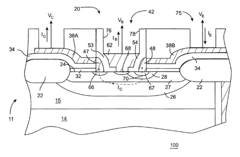
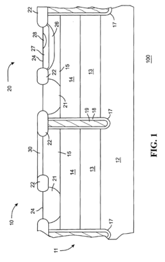
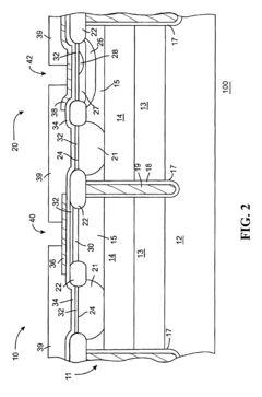
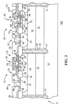
Vertical PNP transistor and method of making same
PatentInactiveUS7972919B2
Innovation
- A method for concurrently forming high-performance vertical PNP and NPN transistors within a single silicon germanium-containing layer using existing processing steps from conventional SiGe BiCMOS technology, aligning the emitter region of the PNP transistor with the intrinsic base region of the NPN transistor, and utilizing low-temperature epitaxial deposition to enhance performance without additional processing steps.


Performance Optimization Strategies for PNP Transistors
Optimizing the performance of PNP transistors is crucial for their effective integration into existing technological frameworks. One key strategy involves careful selection of semiconductor materials. By choosing high-quality, low-defect materials with appropriate bandgap and carrier mobility characteristics, the overall performance of PNP transistors can be significantly enhanced. This includes considering advanced compound semiconductors or engineered silicon-based materials that offer superior electrical properties.
Another critical aspect of performance optimization is the refinement of transistor geometry and structure. Implementing advanced designs such as double-diffused or lateral PNP structures can lead to improved frequency response and current gain. Additionally, optimizing the base width and emitter size can help balance the trade-offs between switching speed and current handling capacity, tailoring the transistor's performance to specific application requirements.
Doping profile optimization plays a vital role in enhancing PNP transistor performance. Precise control over dopant concentrations and gradients in the emitter, base, and collector regions can significantly impact the transistor's electrical characteristics. Advanced doping techniques, such as delta doping or selective epitaxial growth, can be employed to create highly optimized doping profiles that maximize current gain and minimize parasitic capacitances.
Thermal management is another critical factor in PNP transistor performance optimization. Implementing effective heat dissipation strategies, such as improved package designs or the integration of heat spreaders, can help maintain optimal operating temperatures. This is particularly important in high-power applications where thermal effects can significantly impact transistor performance and reliability.
Process optimization and quality control during manufacturing are essential for achieving consistent and high-performance PNP transistors. This includes refining lithography techniques for more precise feature definition, optimizing etching processes for improved surface quality, and implementing stringent contamination control measures. Advanced process control systems and in-line monitoring can help maintain tight tolerances and ensure reproducibility in transistor characteristics.
Lastly, the integration of advanced passivation and isolation techniques can further enhance PNP transistor performance. Implementing high-quality dielectric materials and optimized isolation structures can reduce parasitic capacitances and leakage currents, leading to improved high-frequency performance and overall device efficiency. These strategies, when combined, provide a comprehensive approach to optimizing PNP transistor performance for seamless integration into existing and emerging technological frameworks.
Environmental Impact of PNP Transistor Manufacturing
The manufacturing of PNP transistors, while essential for modern electronics, carries significant environmental implications that warrant careful consideration. The production process involves several stages, each with its own ecological footprint. Initially, the extraction of raw materials, primarily silicon and various dopants, can lead to habitat disruption and resource depletion. Mining activities often result in landscape alterations and potential water pollution if not properly managed.
During the fabrication phase, the creation of PNP transistors requires energy-intensive processes such as crystal growth, wafer slicing, and epitaxial deposition. These procedures consume substantial amounts of electricity, contributing to greenhouse gas emissions if the energy source is not renewable. Additionally, the use of chemicals for etching and cleaning, including hydrofluoric acid and solvents, poses risks of air and water pollution if not handled and disposed of correctly.
The manufacturing process also generates electronic waste (e-waste) in the form of defective wafers, off-spec components, and used chemicals. Proper disposal and recycling of these materials are crucial to prevent soil and groundwater contamination. Moreover, the production of ultra-pure water, essential for semiconductor manufacturing, places a strain on local water resources, particularly in water-scarce regions.
On the positive side, advancements in manufacturing technologies have led to more efficient production methods. Modern fabrication facilities are implementing closed-loop systems for chemical recycling, reducing waste and minimizing environmental impact. Additionally, the trend towards smaller transistor sizes has resulted in more efficient use of materials and energy per unit of computing power.
The semiconductor industry is increasingly adopting green practices, such as utilizing renewable energy sources, implementing stricter waste management protocols, and developing less toxic alternatives to traditional chemicals. These efforts aim to mitigate the environmental impact of PNP transistor production while maintaining technological progress.
As the demand for electronic devices continues to grow, the cumulative environmental effect of transistor manufacturing becomes more pronounced. This necessitates ongoing research into sustainable production methods and materials. Innovations in bio-based semiconductors and recyclable electronics show promise in reducing the long-term ecological footprint of the industry.
In conclusion, while the environmental impact of PNP transistor manufacturing is significant, ongoing technological advancements and industry initiatives are working towards more sustainable practices. Balancing technological progress with environmental stewardship remains a critical challenge for the semiconductor industry.
Unlock deeper insights with PatSnap Eureka Quick Research — get a full tech report to explore trends and direct your research. Try now!
Generate Your Research Report Instantly with AI Agent
Supercharge your innovation with PatSnap Eureka AI Agent Platform!