

How to Utilize AI in Advancing PNP Transistor Efficiency?
JUL 28, 20259 MIN READ
Generate Your Research Report Instantly with AI Agent
PatSnap Eureka helps you evaluate technical feasibility & market potential.
AI-PNP Transistor Background and Objectives
The integration of Artificial Intelligence (AI) with PNP transistor technology represents a significant leap in the field of semiconductor engineering. This convergence aims to enhance the efficiency and performance of PNP transistors, which have been fundamental components in electronic circuits for decades. The evolution of transistor technology has been a cornerstone of the electronics industry, and the application of AI to this domain marks a new frontier in innovation.
Historically, PNP transistors have played a crucial role in analog circuits, power management, and signal amplification. However, as electronic devices become increasingly complex and demand higher performance, traditional approaches to transistor design and optimization have reached their limits. This is where AI enters the picture, offering novel methods to push the boundaries of transistor efficiency.
The primary objective of utilizing AI in advancing PNP transistor efficiency is to optimize various aspects of transistor design, fabrication, and operation. This includes improving parameters such as current gain, switching speed, power consumption, and thermal management. AI algorithms can analyze vast amounts of data from transistor simulations and real-world performance metrics to identify patterns and relationships that human engineers might overlook.
One of the key goals is to develop AI-driven models that can predict transistor behavior under various conditions with unprecedented accuracy. These models can then be used to fine-tune transistor designs, potentially leading to breakthroughs in miniaturization, energy efficiency, and overall performance. Additionally, AI can assist in the development of adaptive transistor systems that can dynamically adjust their characteristics based on real-time operating conditions.
The integration of AI into PNP transistor technology also aims to address manufacturing challenges. Machine learning algorithms can optimize fabrication processes, reduce defects, and increase yield rates. This not only improves the quality of transistors but also contributes to more cost-effective production methods, potentially making advanced transistor technology more accessible across various industries.
Furthermore, the application of AI in this field is expected to accelerate the pace of innovation. By automating certain aspects of the design and testing processes, researchers and engineers can explore a wider range of possibilities in a shorter time frame. This could lead to the discovery of novel transistor architectures or materials that significantly outperform current technologies.
As we look towards the future, the synergy between AI and PNP transistor technology holds promise for enabling next-generation electronic devices. From more efficient power management in mobile devices to advanced control systems in automotive and industrial applications, the potential impact of this technological convergence is vast and far-reaching.
Historically, PNP transistors have played a crucial role in analog circuits, power management, and signal amplification. However, as electronic devices become increasingly complex and demand higher performance, traditional approaches to transistor design and optimization have reached their limits. This is where AI enters the picture, offering novel methods to push the boundaries of transistor efficiency.
The primary objective of utilizing AI in advancing PNP transistor efficiency is to optimize various aspects of transistor design, fabrication, and operation. This includes improving parameters such as current gain, switching speed, power consumption, and thermal management. AI algorithms can analyze vast amounts of data from transistor simulations and real-world performance metrics to identify patterns and relationships that human engineers might overlook.
One of the key goals is to develop AI-driven models that can predict transistor behavior under various conditions with unprecedented accuracy. These models can then be used to fine-tune transistor designs, potentially leading to breakthroughs in miniaturization, energy efficiency, and overall performance. Additionally, AI can assist in the development of adaptive transistor systems that can dynamically adjust their characteristics based on real-time operating conditions.
The integration of AI into PNP transistor technology also aims to address manufacturing challenges. Machine learning algorithms can optimize fabrication processes, reduce defects, and increase yield rates. This not only improves the quality of transistors but also contributes to more cost-effective production methods, potentially making advanced transistor technology more accessible across various industries.
Furthermore, the application of AI in this field is expected to accelerate the pace of innovation. By automating certain aspects of the design and testing processes, researchers and engineers can explore a wider range of possibilities in a shorter time frame. This could lead to the discovery of novel transistor architectures or materials that significantly outperform current technologies.
As we look towards the future, the synergy between AI and PNP transistor technology holds promise for enabling next-generation electronic devices. From more efficient power management in mobile devices to advanced control systems in automotive and industrial applications, the potential impact of this technological convergence is vast and far-reaching.
Market Analysis for AI-Enhanced Transistors
The market for AI-enhanced transistors, particularly PNP transistors, is experiencing significant growth and transformation. As artificial intelligence continues to permeate various industries, the demand for more efficient and intelligent semiconductor components is on the rise. The global market for AI-enhanced transistors is projected to expand rapidly in the coming years, driven by the increasing adoption of AI technologies across diverse sectors.
The automotive industry represents a key market for AI-enhanced PNP transistors. With the growing trend towards electric and autonomous vehicles, there is a heightened need for advanced power management and signal processing capabilities. AI-enhanced PNP transistors can offer improved efficiency and performance in these applications, contributing to extended battery life and enhanced vehicle intelligence.
In the consumer electronics sector, the demand for AI-enhanced transistors is also surging. Smartphones, wearables, and smart home devices are increasingly incorporating AI functionalities, necessitating more sophisticated and energy-efficient transistor technologies. PNP transistors optimized through AI can enable longer battery life, faster processing speeds, and improved overall performance in these devices.
The industrial automation sector presents another significant market opportunity for AI-enhanced PNP transistors. As factories and manufacturing processes become more intelligent and interconnected, there is a growing need for advanced semiconductor components that can support AI-driven decision-making and control systems. AI-optimized PNP transistors can contribute to improved energy efficiency, reduced downtime, and enhanced productivity in industrial settings.
The telecommunications industry is also a key driver of demand for AI-enhanced transistors. With the ongoing rollout of 5G networks and the increasing complexity of communication systems, there is a need for more efficient and intelligent semiconductor components. AI-enhanced PNP transistors can play a crucial role in improving signal processing, power management, and overall network performance.
In the healthcare sector, the integration of AI technologies is creating new opportunities for advanced transistor applications. Medical devices, diagnostic equipment, and wearable health monitors are increasingly relying on AI capabilities, driving demand for more efficient and reliable semiconductor components. AI-enhanced PNP transistors can contribute to improved accuracy, reduced power consumption, and enhanced performance in these critical healthcare applications.
The market landscape for AI-enhanced transistors is characterized by intense competition and rapid technological advancements. Major semiconductor manufacturers are investing heavily in research and development to create more efficient and intelligent transistor designs. Startups and research institutions are also contributing to innovation in this space, exploring novel approaches to integrating AI capabilities into transistor technologies.
The automotive industry represents a key market for AI-enhanced PNP transistors. With the growing trend towards electric and autonomous vehicles, there is a heightened need for advanced power management and signal processing capabilities. AI-enhanced PNP transistors can offer improved efficiency and performance in these applications, contributing to extended battery life and enhanced vehicle intelligence.
In the consumer electronics sector, the demand for AI-enhanced transistors is also surging. Smartphones, wearables, and smart home devices are increasingly incorporating AI functionalities, necessitating more sophisticated and energy-efficient transistor technologies. PNP transistors optimized through AI can enable longer battery life, faster processing speeds, and improved overall performance in these devices.
The industrial automation sector presents another significant market opportunity for AI-enhanced PNP transistors. As factories and manufacturing processes become more intelligent and interconnected, there is a growing need for advanced semiconductor components that can support AI-driven decision-making and control systems. AI-optimized PNP transistors can contribute to improved energy efficiency, reduced downtime, and enhanced productivity in industrial settings.
The telecommunications industry is also a key driver of demand for AI-enhanced transistors. With the ongoing rollout of 5G networks and the increasing complexity of communication systems, there is a need for more efficient and intelligent semiconductor components. AI-enhanced PNP transistors can play a crucial role in improving signal processing, power management, and overall network performance.
In the healthcare sector, the integration of AI technologies is creating new opportunities for advanced transistor applications. Medical devices, diagnostic equipment, and wearable health monitors are increasingly relying on AI capabilities, driving demand for more efficient and reliable semiconductor components. AI-enhanced PNP transistors can contribute to improved accuracy, reduced power consumption, and enhanced performance in these critical healthcare applications.
The market landscape for AI-enhanced transistors is characterized by intense competition and rapid technological advancements. Major semiconductor manufacturers are investing heavily in research and development to create more efficient and intelligent transistor designs. Startups and research institutions are also contributing to innovation in this space, exploring novel approaches to integrating AI capabilities into transistor technologies.
Current AI Integration in Transistor Technology
Artificial Intelligence (AI) has made significant inroads into transistor technology, revolutionizing the design, optimization, and manufacturing processes of PNP transistors. Machine learning algorithms are now being employed to analyze vast amounts of data generated during transistor production, enabling manufacturers to identify patterns and optimize performance parameters with unprecedented accuracy.
One of the key areas where AI is making a substantial impact is in the realm of predictive modeling. Advanced neural networks are being utilized to simulate transistor behavior under various operating conditions, allowing engineers to fine-tune designs without the need for extensive physical prototyping. This approach not only accelerates the development cycle but also leads to more efficient and reliable PNP transistors.
In the field of process control, AI-driven systems are being implemented to monitor and adjust manufacturing parameters in real-time. These intelligent systems can detect minute variations in production conditions and make instantaneous adjustments to maintain optimal transistor characteristics. This level of precision control was previously unattainable with traditional manufacturing methods.
AI is also playing a crucial role in defect detection and quality control. Computer vision algorithms, coupled with deep learning models, are being used to inspect transistors at various stages of production. These systems can identify defects with a higher degree of accuracy than human inspectors, ensuring that only high-quality PNP transistors reach the market.
Furthermore, AI is being leveraged to optimize the layout and design of integrated circuits that incorporate PNP transistors. Generative design algorithms can explore countless iterations of circuit layouts, proposing novel configurations that maximize efficiency and minimize power consumption. This approach is particularly valuable in the development of high-performance, low-power electronic devices.
In the realm of materials science, AI is assisting researchers in discovering new semiconductor materials and doping techniques that could potentially enhance PNP transistor efficiency. Machine learning models are being used to predict the properties of novel materials, accelerating the discovery process and potentially leading to breakthroughs in transistor technology.
Lastly, AI is being employed in the optimization of transistor packaging and thermal management. Computational fluid dynamics simulations, guided by machine learning algorithms, are helping engineers design more effective cooling solutions for high-power transistor applications. This integration of AI in thermal design is crucial for pushing the boundaries of transistor performance while maintaining reliability.
One of the key areas where AI is making a substantial impact is in the realm of predictive modeling. Advanced neural networks are being utilized to simulate transistor behavior under various operating conditions, allowing engineers to fine-tune designs without the need for extensive physical prototyping. This approach not only accelerates the development cycle but also leads to more efficient and reliable PNP transistors.
In the field of process control, AI-driven systems are being implemented to monitor and adjust manufacturing parameters in real-time. These intelligent systems can detect minute variations in production conditions and make instantaneous adjustments to maintain optimal transistor characteristics. This level of precision control was previously unattainable with traditional manufacturing methods.
AI is also playing a crucial role in defect detection and quality control. Computer vision algorithms, coupled with deep learning models, are being used to inspect transistors at various stages of production. These systems can identify defects with a higher degree of accuracy than human inspectors, ensuring that only high-quality PNP transistors reach the market.
Furthermore, AI is being leveraged to optimize the layout and design of integrated circuits that incorporate PNP transistors. Generative design algorithms can explore countless iterations of circuit layouts, proposing novel configurations that maximize efficiency and minimize power consumption. This approach is particularly valuable in the development of high-performance, low-power electronic devices.
In the realm of materials science, AI is assisting researchers in discovering new semiconductor materials and doping techniques that could potentially enhance PNP transistor efficiency. Machine learning models are being used to predict the properties of novel materials, accelerating the discovery process and potentially leading to breakthroughs in transistor technology.
Lastly, AI is being employed in the optimization of transistor packaging and thermal management. Computational fluid dynamics simulations, guided by machine learning algorithms, are helping engineers design more effective cooling solutions for high-power transistor applications. This integration of AI in thermal design is crucial for pushing the boundaries of transistor performance while maintaining reliability.
AI Techniques for PNP Transistor Optimization
01 Structural improvements for PNP transistor efficiency
Various structural modifications can enhance PNP transistor efficiency. These include optimizing the base-emitter junction, improving the collector design, and refining the overall transistor geometry. Such improvements can lead to reduced parasitic capacitances, lower power consumption, and increased switching speeds.- Improved PNP transistor structure: Enhancements in PNP transistor design focus on optimizing the structure to improve efficiency. This includes modifications to the base, emitter, and collector regions, as well as the use of advanced materials and fabrication techniques to reduce parasitic capacitances and improve current gain.
- Biasing techniques for PNP transistors: Efficient biasing methods are crucial for optimizing PNP transistor performance. These techniques involve careful selection of operating points, voltage levels, and current sources to maximize gain, minimize power consumption, and ensure stable operation across various temperature ranges and operating conditions.
- Integration of PNP transistors in IC design: Integrating PNP transistors effectively in integrated circuit designs is key to overall system efficiency. This involves optimizing layout, reducing parasitic effects, and implementing circuit topologies that leverage the unique characteristics of PNP transistors to enhance performance in analog and mixed-signal applications.
- Temperature compensation in PNP transistors: Implementing temperature compensation techniques is crucial for maintaining PNP transistor efficiency across varying environmental conditions. This includes designing circuits with temperature-independent biasing, using complementary NPN-PNP pairs, and incorporating temperature sensing and feedback mechanisms to adjust operating parameters dynamically.
- High-frequency performance optimization: Enhancing the high-frequency performance of PNP transistors is essential for their use in modern high-speed applications. This involves reducing parasitic capacitances, optimizing device geometry, and implementing advanced fabrication techniques to improve cut-off frequency and switching speed while maintaining high current gain.
02 Doping techniques for enhanced PNP transistor performance
Advanced doping methods can significantly improve PNP transistor efficiency. Techniques such as selective doping, gradient doping profiles, and precise control of impurity concentrations in different regions of the transistor can optimize carrier mobility, reduce resistance, and enhance overall transistor performance.Expand Specific Solutions03 Circuit design strategies for efficient PNP transistor utilization
Innovative circuit designs can maximize PNP transistor efficiency in various applications. This includes developing specialized biasing circuits, implementing feedback mechanisms, and optimizing load conditions. Such circuit-level approaches can improve power efficiency, reduce noise, and enhance overall system performance.Expand Specific Solutions04 Integration techniques for high-efficiency PNP transistors
Advanced integration methods can improve PNP transistor efficiency in complex semiconductor devices. This involves optimizing the transistor's placement within integrated circuits, minimizing parasitic effects, and ensuring compatibility with other components. Such integration techniques can lead to better overall chip performance and reduced power consumption.Expand Specific Solutions05 Temperature compensation and stability enhancements for PNP transistors
Implementing temperature compensation techniques and stability enhancements can improve PNP transistor efficiency across varying operating conditions. This includes developing specialized bias circuits, utilizing temperature-sensitive components, and optimizing the transistor structure for thermal stability. These approaches can lead to more consistent performance and improved reliability in different environments.Expand Specific Solutions
Key Players in AI-Transistor Development
The AI-driven advancement of PNP transistor efficiency is in a nascent stage, with significant potential for market growth as the technology matures. The competitive landscape is characterized by a mix of established semiconductor giants and innovative research institutions. Companies like IBM, QUALCOMM, and Intel are leveraging their extensive R&D capabilities to explore AI applications in transistor design. Meanwhile, specialized firms such as Semiconductor Energy Laboratory and GLOBALFOUNDRIES are focusing on novel materials and fabrication techniques. Academic institutions like Fudan University and Northwestern University are contributing fundamental research. As the field evolves, collaborations between industry leaders and research centers are likely to accelerate progress, driving both technological advancements and market expansion.
International Business Machines Corp.
Technical Solution: IBM is leveraging AI to enhance PNP transistor efficiency through several innovative approaches. They are using machine learning algorithms to optimize transistor design parameters, such as doping profiles, gate dimensions, and material compositions. IBM's AI-driven simulation tools can predict transistor performance with high accuracy, reducing the need for time-consuming physical prototyping[1]. The company has also developed AI models that can analyze vast amounts of manufacturing data to identify subtle patterns affecting transistor efficiency, enabling real-time process adjustments[2]. Additionally, IBM is exploring the use of quantum computing in conjunction with AI to solve complex optimization problems in transistor design, potentially leading to breakthrough improvements in PNP transistor efficiency[3].
Strengths: Extensive experience in semiconductor technology, access to advanced AI and quantum computing resources. Weaknesses: High development costs, potential challenges in scaling AI solutions to mass production.
QUALCOMM, Inc.
Technical Solution: Qualcomm is applying AI to enhance PNP transistor efficiency in several innovative ways. They are using machine learning algorithms to optimize transistor design for mobile and IoT applications, focusing on power efficiency and performance[1]. Qualcomm's AI models analyze complex interactions between transistor parameters and system-level performance, enabling holistic optimization of chip designs[2]. The company has developed AI-driven simulation tools that can accurately predict transistor behavior under various operating conditions, significantly reducing design iteration time[3]. Additionally, Qualcomm is exploring the use of AI in adaptive power management systems that can dynamically adjust transistor operating points based on real-time workload and environmental factors, further improving overall efficiency[4].
Strengths: Strong focus on mobile and IoT applications, expertise in low-power design. Weaknesses: Narrower focus compared to general semiconductor manufacturers, potential limitations in applying solutions to non-mobile sectors.
Innovative AI Algorithms for Transistor Design
Information processing system, information processing method, program, and substrate processing apparatus
PatentActiveUS20220093409A1
Innovation
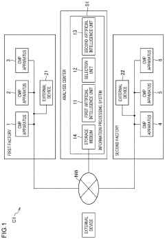
- An information processing system utilizing artificial intelligence units to learn from datasets, predict performance values, and select optimal parameter combinations based on correlation analysis, allowing for the adjustment of multiple parameters to enhance the performance of the CMP apparatus.


Environmental Impact of AI-Optimized Transistors
The environmental impact of AI-optimized PNP transistors is a crucial consideration in the advancement of semiconductor technology. As artificial intelligence techniques are increasingly applied to enhance transistor efficiency, the resulting improvements in performance and energy consumption have significant implications for the environment. AI-driven optimization of PNP transistors can lead to reduced power consumption, which translates to lower energy requirements for electronic devices and systems. This reduction in energy demand has a cascading effect on the overall carbon footprint of the technology sector.
The manufacturing process of AI-optimized transistors also plays a role in their environmental impact. Advanced AI algorithms can help streamline production processes, potentially reducing waste and improving resource utilization. By optimizing the design and fabrication of PNP transistors, AI can contribute to more efficient use of raw materials, potentially decreasing the environmental burden associated with semiconductor manufacturing.
Furthermore, the increased efficiency of AI-optimized PNP transistors can extend the lifespan of electronic devices. This longevity can lead to a reduction in electronic waste, addressing one of the most pressing environmental challenges in the technology industry. As devices become more energy-efficient and durable, the need for frequent replacements diminishes, potentially slowing down the cycle of electronic consumption and disposal.
However, it is important to consider the environmental cost of developing and implementing AI systems for transistor optimization. The training and operation of complex AI models require significant computational resources, which in turn consume energy. This raises questions about the net environmental benefit of AI-optimized transistors, necessitating a comprehensive life cycle assessment to fully understand their ecological impact.
The potential for AI to enable more sophisticated power management in electronic systems is another aspect to consider. AI-optimized PNP transistors could facilitate more dynamic and responsive power control, further reducing energy waste in various applications. This could have far-reaching effects on the energy efficiency of data centers, mobile devices, and other technology-dependent sectors.
In conclusion, while AI-optimized PNP transistors show promise in reducing the environmental footprint of electronic devices, a holistic approach is necessary to fully assess their impact. The benefits of improved efficiency and reduced energy consumption must be weighed against the environmental costs of AI development and implementation. As research in this field progresses, it will be crucial to prioritize sustainable practices in both the optimization process and the lifecycle management of AI-enhanced semiconductor technologies.
The manufacturing process of AI-optimized transistors also plays a role in their environmental impact. Advanced AI algorithms can help streamline production processes, potentially reducing waste and improving resource utilization. By optimizing the design and fabrication of PNP transistors, AI can contribute to more efficient use of raw materials, potentially decreasing the environmental burden associated with semiconductor manufacturing.
Furthermore, the increased efficiency of AI-optimized PNP transistors can extend the lifespan of electronic devices. This longevity can lead to a reduction in electronic waste, addressing one of the most pressing environmental challenges in the technology industry. As devices become more energy-efficient and durable, the need for frequent replacements diminishes, potentially slowing down the cycle of electronic consumption and disposal.
However, it is important to consider the environmental cost of developing and implementing AI systems for transistor optimization. The training and operation of complex AI models require significant computational resources, which in turn consume energy. This raises questions about the net environmental benefit of AI-optimized transistors, necessitating a comprehensive life cycle assessment to fully understand their ecological impact.
The potential for AI to enable more sophisticated power management in electronic systems is another aspect to consider. AI-optimized PNP transistors could facilitate more dynamic and responsive power control, further reducing energy waste in various applications. This could have far-reaching effects on the energy efficiency of data centers, mobile devices, and other technology-dependent sectors.
In conclusion, while AI-optimized PNP transistors show promise in reducing the environmental footprint of electronic devices, a holistic approach is necessary to fully assess their impact. The benefits of improved efficiency and reduced energy consumption must be weighed against the environmental costs of AI development and implementation. As research in this field progresses, it will be crucial to prioritize sustainable practices in both the optimization process and the lifecycle management of AI-enhanced semiconductor technologies.
Ethical Considerations in AI-Transistor Research
As the field of AI-driven transistor research advances, it becomes increasingly important to address the ethical considerations surrounding this technology. The integration of AI in PNP transistor efficiency optimization raises several ethical concerns that must be carefully examined and addressed.
One primary ethical consideration is the potential for job displacement in the semiconductor industry. As AI systems become more proficient in designing and optimizing transistors, there is a risk that human engineers and technicians may be replaced by automated processes. This could lead to significant workforce disruptions and economic challenges for individuals and communities reliant on the semiconductor industry.
Privacy and data security also emerge as critical ethical issues in AI-transistor research. The development of more efficient PNP transistors through AI may require vast amounts of data, including proprietary information from various semiconductor companies. Ensuring the protection of this sensitive data and maintaining fair competition in the industry becomes paramount.
The environmental impact of AI-driven transistor research is another ethical concern. While AI may lead to more energy-efficient transistors, the computational resources required for AI model training and operation could potentially offset these gains. Balancing the environmental benefits of improved transistor efficiency against the ecological footprint of AI systems is crucial.
Bias and fairness in AI algorithms used for transistor optimization must also be addressed. If the training data or algorithms contain inherent biases, it could lead to suboptimal or unfair design outcomes, potentially favoring certain types of transistors or applications over others. Ensuring diversity in both the AI development teams and the data used for training is essential to mitigate these risks.
The potential dual-use nature of advanced AI-optimized transistors raises ethical questions about their applications. While improved transistor efficiency can benefit numerous fields, including healthcare and renewable energy, these same advancements could also be applied to military or surveillance technologies. Researchers and organizations must carefully consider the potential consequences of their work and implement safeguards to prevent misuse.
Transparency and explainability in AI-driven transistor design processes are crucial ethical considerations. As AI systems become more complex, it may become increasingly difficult for human engineers to understand and validate the decisions made by these systems. Ensuring that AI-generated designs can be explained and verified is essential for maintaining trust and accountability in the industry.
One primary ethical consideration is the potential for job displacement in the semiconductor industry. As AI systems become more proficient in designing and optimizing transistors, there is a risk that human engineers and technicians may be replaced by automated processes. This could lead to significant workforce disruptions and economic challenges for individuals and communities reliant on the semiconductor industry.
Privacy and data security also emerge as critical ethical issues in AI-transistor research. The development of more efficient PNP transistors through AI may require vast amounts of data, including proprietary information from various semiconductor companies. Ensuring the protection of this sensitive data and maintaining fair competition in the industry becomes paramount.
The environmental impact of AI-driven transistor research is another ethical concern. While AI may lead to more energy-efficient transistors, the computational resources required for AI model training and operation could potentially offset these gains. Balancing the environmental benefits of improved transistor efficiency against the ecological footprint of AI systems is crucial.
Bias and fairness in AI algorithms used for transistor optimization must also be addressed. If the training data or algorithms contain inherent biases, it could lead to suboptimal or unfair design outcomes, potentially favoring certain types of transistors or applications over others. Ensuring diversity in both the AI development teams and the data used for training is essential to mitigate these risks.
The potential dual-use nature of advanced AI-optimized transistors raises ethical questions about their applications. While improved transistor efficiency can benefit numerous fields, including healthcare and renewable energy, these same advancements could also be applied to military or surveillance technologies. Researchers and organizations must carefully consider the potential consequences of their work and implement safeguards to prevent misuse.
Transparency and explainability in AI-driven transistor design processes are crucial ethical considerations. As AI systems become more complex, it may become increasingly difficult for human engineers to understand and validate the decisions made by these systems. Ensuring that AI-generated designs can be explained and verified is essential for maintaining trust and accountability in the industry.
Unlock deeper insights with PatSnap Eureka Quick Research — get a full tech report to explore trends and direct your research. Try now!
Generate Your Research Report Instantly with AI Agent
Supercharge your innovation with PatSnap Eureka AI Agent Platform!