How To Evaluate FinFET Operational Current
SEP 11, 20259 MIN READ
Generate Your Research Report Instantly with AI Agent
PatSnap Eureka helps you evaluate technical feasibility & market potential.
FinFET Current Evaluation Background and Objectives
The evolution of semiconductor technology has witnessed a significant paradigm shift with the introduction of FinFET (Fin Field-Effect Transistor) architecture, which emerged as a response to the scaling limitations of traditional planar MOSFETs. Since its commercial introduction in 2011, FinFET technology has become the cornerstone of advanced semiconductor manufacturing processes, enabling continued adherence to Moore's Law despite increasing physical constraints.
Current evaluation in FinFET devices represents a critical aspect of semiconductor performance assessment, directly impacting power consumption, switching speed, and overall circuit reliability. The three-dimensional nature of FinFET structures introduces unique challenges in current measurement and characterization that were not present in planar technologies, necessitating new evaluation methodologies and standards.
Historically, current evaluation techniques have evolved from simple DC measurements to sophisticated multi-parameter analyses that account for quantum effects, short-channel phenomena, and thermal considerations. The industry has progressively refined these techniques to address the increasing complexity of FinFET geometries across successive technology nodes, from 22nm to the current sub-7nm processes.
The primary objective of FinFET operational current evaluation is to accurately characterize device performance under various operating conditions, enabling precise modeling for circuit design and optimization. This includes quantifying on-state current (ION), off-state leakage (IOFF), subthreshold swing, and drain-induced barrier lowering (DIBL) effects, which collectively determine the efficiency and reliability of FinFET-based integrated circuits.
Additionally, current evaluation aims to establish standardized methodologies that facilitate meaningful comparisons between different FinFET technologies and manufacturing processes. This standardization is essential for benchmarking purposes and for guiding future technology development decisions across the semiconductor industry.
Another critical goal is to develop predictive models that can accurately forecast FinFET current characteristics during the design phase, reducing the need for costly fabrication iterations. These models must account for process variations, environmental factors, and aging effects to ensure reliable long-term operation of FinFET-based systems.
As FinFET technology continues to evolve toward gate-all-around (GAA) structures and other novel architectures, current evaluation techniques must similarly advance to address emerging challenges such as quantum confinement effects, ballistic transport, and increased variability at atomic scales. The trajectory of this technological evolution will significantly influence future evaluation methodologies and performance metrics.
Market Demand Analysis for FinFET Technology
The FinFET technology market has experienced substantial growth since its commercial introduction in 2011, driven primarily by the semiconductor industry's need for more efficient transistor architectures at advanced process nodes. Current market analysis indicates that the global FinFET technology market reached approximately $45 billion in 2022, with projections suggesting a compound annual growth rate (CAGR) of 22% through 2028.
The demand for accurate FinFET operational current evaluation stems from multiple industry sectors. Semiconductor manufacturers require precise current measurement methodologies to optimize chip performance and power efficiency. This need has intensified as node sizes have decreased from 22nm to the current 3nm processes, with each generation demanding more sophisticated evaluation techniques.
Mobile device manufacturers represent the largest market segment utilizing FinFET technology, accounting for roughly 38% of the total market share. Their demand for longer battery life and higher performance in smaller form factors directly translates to requirements for precise operational current evaluation. The automotive sector follows as the fastest-growing segment with 29% year-over-year growth, driven by the increasing semiconductor content in vehicles and stringent reliability requirements.
Data centers and high-performance computing applications constitute another significant market driver, representing approximately 25% of the current FinFET market. These applications demand extreme power efficiency at maximum performance, making accurate operational current evaluation critical for competitive product development.
Industry surveys indicate that 76% of semiconductor design houses consider operational current evaluation as "extremely important" in their development process, with 89% reporting increased investment in related testing equipment and methodologies over the past three years.
Geographically, Asia-Pacific dominates the market with 62% share, led by Taiwan, South Korea, and increasingly China. North America follows with 24%, while Europe accounts for 12% of the global market. The concentration of foundries in Asia-Pacific explains this regional distribution, though research activities remain more globally distributed.
The market for specialized equipment and software tools for FinFET current evaluation has emerged as a distinct sub-segment, growing at 18% annually and currently valued at approximately $3.2 billion. This includes advanced probe systems, parameter analyzers, and simulation software specifically designed for nanoscale current measurements.
Current Challenges in FinFET Operational Current Measurement
Despite significant advancements in FinFET technology, measuring operational current in these devices presents several complex challenges that impact both research and manufacturing environments. The three-dimensional structure of FinFETs, while beneficial for performance, creates inherent difficulties in obtaining accurate current measurements compared to planar transistors.
One primary challenge is the variability in fin dimensions and geometry. Even minor variations in fin height, width, or sidewall angle can significantly alter current flow characteristics. Manufacturing processes typically produce fins with dimensional variations of 1-2nm, which can translate to current variations exceeding 10% between supposedly identical devices, complicating standardized measurement protocols.
The quantum confinement effects in FinFETs further complicate current measurement. As fin widths approach sub-10nm dimensions, quantum mechanical effects become increasingly prominent, causing deviations from classical current-voltage relationships. These effects create non-linear behaviors that traditional measurement techniques struggle to characterize accurately, particularly at low operational voltages.
Temperature dependence presents another significant challenge. FinFET operational current exhibits stronger temperature sensitivity than planar devices due to their unique geometry and confined channel structure. This necessitates precise temperature control during measurements, typically requiring stability within ±0.1°C to ensure reproducible results, which is difficult to maintain in high-volume testing environments.
Parasitic resistances and capacitances in FinFET structures significantly impact current measurement accuracy. The complex interconnect structures and multiple gates create additional resistive and capacitive elements that can mask the intrinsic device performance. Separating these parasitic effects from actual channel current requires sophisticated de-embedding techniques that add complexity to measurement systems.
Contact resistance variability between the measurement equipment and device terminals introduces another layer of uncertainty. The reduced contact areas in advanced FinFET nodes make reliable, low-resistance connections increasingly difficult to establish. This variability can account for measurement discrepancies of up to 15% between identical devices, particularly problematic when characterizing low-current operations.
Finally, the industry faces challenges in measurement standardization. Different equipment manufacturers employ varying methodologies for current measurement in FinFETs, leading to inconsistencies when comparing results across platforms. The lack of universally accepted measurement protocols specifically designed for FinFET structures hampers cross-validation of research findings and manufacturing quality control processes.
Mainstream FinFET Current Evaluation Techniques
01 FinFET structure optimization for current control
Structural modifications to FinFET designs can significantly impact operational current characteristics. These modifications include adjusting fin height, width, and spacing to optimize current flow. Multi-fin configurations and gate length variations can be implemented to achieve desired current densities while maintaining thermal stability. These structural optimizations help balance performance requirements with power consumption constraints in advanced semiconductor applications.- FinFET structure optimization for current control: Optimizing the physical structure of FinFETs can significantly impact operational current characteristics. This includes modifications to fin height, width, and shape, as well as gate length and oxide thickness. These structural optimizations can enhance current drive capability while maintaining low leakage current, improving overall device performance and power efficiency in integrated circuits.
- Multi-threshold voltage techniques for FinFET current management: Implementing multiple threshold voltage designs in FinFET devices allows for precise control of operational current. By utilizing different doping profiles, gate materials, or work function metals, manufacturers can create FinFETs with varying threshold voltages on the same chip. This approach enables optimization of both high-performance (high current) and low-power (low current) operations in different circuit sections.
- Dynamic current control in FinFET circuits: Dynamic current control mechanisms in FinFET-based circuits allow for adaptive power management. These techniques include body biasing, adaptive voltage scaling, and clock gating specifically designed for FinFET architectures. By dynamically adjusting operational current based on processing demands, these approaches can significantly reduce power consumption while maintaining performance when needed.
- FinFET current sensing and measurement techniques: Specialized techniques for accurately sensing and measuring operational current in FinFET devices are essential for both testing and operational management. These include on-chip current sensors, specialized test structures, and measurement methodologies that account for the three-dimensional nature of FinFETs. Accurate current measurement enables better characterization, binning, and quality control of FinFET devices.
- FinFET circuit design for optimal current efficiency: Circuit design techniques specifically tailored for FinFET technology can optimize operational current efficiency. These include specialized logic families, memory cell designs, and analog circuits that leverage the unique characteristics of FinFETs. By accounting for the three-dimensional channel structure and improved electrostatic control, these design approaches can achieve better performance-to-power ratios than traditional planar CMOS designs.
02 Threshold voltage management in FinFET devices
Threshold voltage management techniques are crucial for controlling operational current in FinFET devices. By adjusting channel doping profiles, gate work function materials, and implementing multi-threshold voltage designs, manufacturers can precisely tune the current characteristics. Advanced threshold voltage management enables optimization of static and dynamic power consumption while maintaining performance targets across various operating conditions.Expand Specific Solutions03 Power management techniques for FinFET operational current
Various power management techniques can be employed to control operational current in FinFET devices. These include dynamic voltage and frequency scaling, power gating, and body biasing. Implementing sleep modes and standby current reduction techniques helps minimize leakage current while maintaining performance during active operation. Advanced power management controllers can dynamically adjust operational parameters based on workload requirements.Expand Specific Solutions04 Circuit design considerations for FinFET current optimization
Circuit-level design strategies significantly impact FinFET operational current characteristics. Techniques such as transistor sizing, stack forcing, and logic restructuring can be employed to optimize current flow. Specialized circuit topologies that leverage the three-dimensional nature of FinFETs can reduce parasitic effects and improve current efficiency. Consideration of interconnect resistance and capacitance is also crucial for maintaining desired current characteristics in complex integrated circuits.Expand Specific Solutions05 Temperature and process variation effects on FinFET current
Temperature fluctuations and manufacturing process variations significantly impact FinFET operational current. Compensation techniques such as adaptive body biasing and temperature-aware design methodologies can mitigate these effects. Self-adjusting circuits that monitor and respond to temperature changes help maintain consistent current characteristics across operating conditions. Statistical design approaches account for process variations to ensure reliable current performance across manufactured devices.Expand Specific Solutions
Key Industry Players in FinFET Technology
The FinFET operational current evaluation landscape is currently in a mature growth phase, with the market expanding rapidly due to increasing demand for high-performance, energy-efficient semiconductor devices. Leading players in this technical domain include TSMC, GlobalFoundries, and SMIC, who have established sophisticated evaluation methodologies for FinFET current characteristics. The technology has reached commercial maturity with 7nm and 5nm nodes widely deployed, though research continues for sub-5nm applications. Companies like IBM, IMEC, and Qualcomm are driving innovation in measurement techniques and simulation tools, while foundries such as UMC and SMIC are working to optimize current evaluation methods for manufacturing efficiency. The competitive landscape reflects both established semiconductor giants and specialized research institutions collaborating to advance FinFET performance evaluation capabilities.
Semiconductor Manufacturing International (Shanghai) Corp.
Technical Solution: SMIC has developed a systematic approach for evaluating FinFET operational current focusing on their 14nm and 12nm FinFET processes. Their methodology incorporates specialized test structures with varying fin dimensions to isolate electrostatic effects on current flow. SMIC employs a combination of direct current measurements and capacitance-voltage techniques to characterize carrier transport mechanisms. Their evaluation process includes temperature-dependent measurements (typically from -40°C to 125°C) to extract activation energies and understand thermal effects on operational current. SMIC has implemented advanced parameter extraction algorithms that account for series resistance effects and mobility degradation specific to their FinFET architecture. Their approach includes statistical analysis across multiple wafers and lots to establish process corners and ensure manufacturing consistency of current characteristics[2]. SMIC also utilizes specialized techniques to evaluate parasitic components that affect operational current, including source/drain resistance and gate-induced drain leakage (GIDL)[4].
Strengths: Well-established methodology for evaluating process variations' impact on operational current; strong focus on manufacturing consistency across wafers. Weaknesses: Less mature FinFET technology compared to industry leaders; evaluation methods may not fully capture quantum effects at advanced nodes below 10nm.
Taiwan Semiconductor Manufacturing Co., Ltd.
Technical Solution: TSMC employs a comprehensive approach to evaluate FinFET operational current through advanced characterization techniques. Their methodology includes multi-temperature current-voltage (I-V) measurements across different bias conditions to extract key parameters like threshold voltage and subthreshold swing. TSMC utilizes specialized test structures with varying fin widths and heights to isolate and quantify the contributions of different current components. Their evaluation process incorporates both DC and AC current measurements, with particular focus on the relationship between gate voltage and drain current (Id-Vg) to assess carrier mobility and channel resistance. TSMC has developed proprietary simulation models that account for quantum confinement effects and short-channel effects specific to their FinFET technology nodes (5nm and below)[1]. Their evaluation methodology also includes reliability assessment through hot carrier injection (HCI) and bias temperature instability (BTI) tests to understand operational current degradation over device lifetime[3].
Strengths: Industry-leading metrology capabilities with sub-nanometer precision for accurate current measurements; extensive database of historical measurements enabling comparative analysis across technology nodes. Weaknesses: Their evaluation methods are optimized for high-performance computing applications and may not fully address ultra-low power scenarios; proprietary nature of some measurement techniques limits academic validation.
Critical Patents and Literature on FinFET Current Measurement
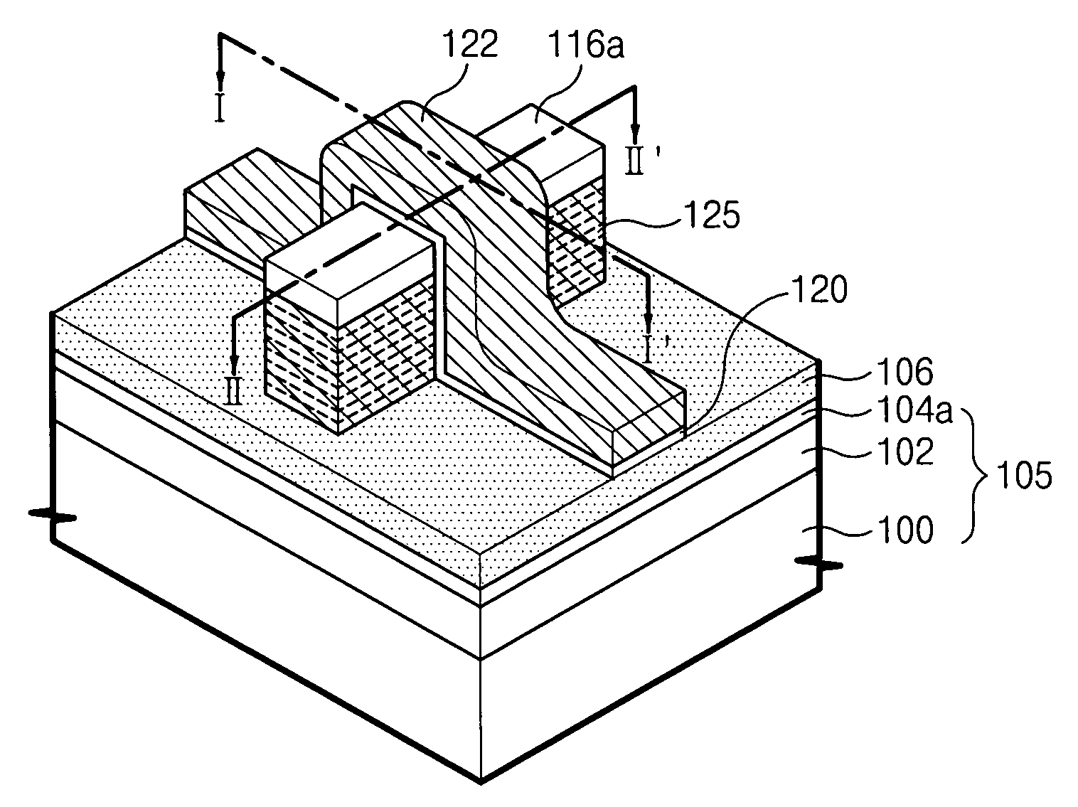
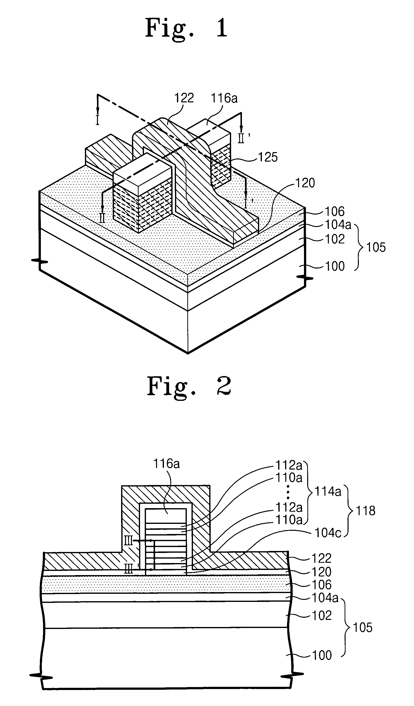
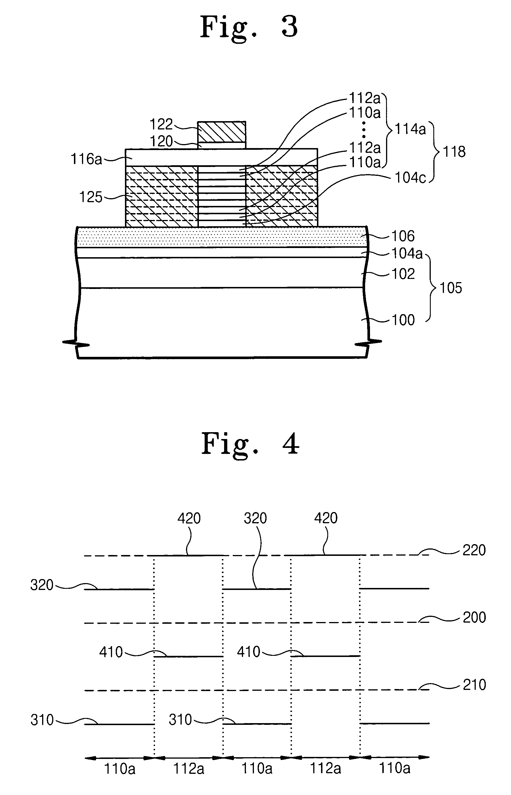
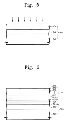
Fin field effect transistors having multi-layer fin patterns
PatentActiveUS7323710B2
Innovation
- The Fin FET design incorporates a fin pattern with stacked semiconductor patterns of strained silicon and silicon-germanium, where the lattice widths of these patterns are greater than the substrate material, reducing stress and increasing the height of the fin pattern, and includes a buffer semiconductor layer and a relaxed semiconductor layer to enhance carrier mobility and on-current.
Contact formation through low-tempearature epitaxial deposition in semiconductor devices
PatentActiveUS20190148377A1
Innovation
- A method involving low-temperature epitaxial deposition of semiconductor material layers, implantation of elements to form amorphous layers, and subsequent annealing to create metastable alloy layers, followed by metal liner deposition and annealing to form metal-semiconductor compounds, which reduces contact resistance and improves the surface condition of the trench.


Power Efficiency Considerations in FinFET Design
Power efficiency has become a critical factor in FinFET design as semiconductor technology continues to advance toward smaller nodes. The operational current of FinFETs directly impacts power consumption, making its evaluation essential for optimizing energy efficiency in modern integrated circuits. When evaluating FinFET operational current for power efficiency, designers must consider both static and dynamic power components.
Static power consumption, primarily resulting from leakage currents, represents a significant challenge in FinFET designs. The three-dimensional structure of FinFETs offers inherent advantages in reducing short-channel effects and gate leakage compared to planar transistors. However, proper evaluation of subthreshold leakage and gate-induced drain leakage (GIDL) remains crucial for minimizing static power consumption.
Dynamic power consumption, proportional to switching frequency and the square of supply voltage, demands careful consideration of FinFET operational current characteristics. The capacitive load charging and discharging during switching operations constitutes the majority of dynamic power consumption. Evaluating the current-voltage (I-V) characteristics across different operating conditions provides essential insights for optimizing dynamic power efficiency.
Temperature effects significantly influence FinFET operational current and consequently power efficiency. As temperature increases, carrier mobility decreases while leakage current increases exponentially. Comprehensive evaluation methodologies must include temperature-dependent current measurements to ensure power efficiency across the entire operating temperature range of the target application.
Supply voltage scaling represents one of the most effective approaches for improving power efficiency in FinFET designs. However, reducing supply voltage impacts performance metrics such as switching speed and noise margins. Evaluating the operational current at various supply voltages helps identify the optimal voltage point that balances power consumption and performance requirements.
Multi-threshold voltage (multi-Vt) design techniques offer another dimension for power optimization. By employing different threshold voltages for transistors based on their timing criticality, designers can reduce leakage power while maintaining performance in critical paths. Accurate evaluation of operational current across different threshold voltage options is essential for effective implementation of multi-Vt strategies.
Advanced power management techniques, including power gating and dynamic voltage and frequency scaling (DVFS), rely on precise characterization of FinFET operational current. These techniques dynamically adjust power consumption based on workload demands, making accurate current evaluation across various operating modes crucial for maximizing energy efficiency in modern semiconductor devices.
Reliability Testing Standards for FinFET Devices
Reliability testing standards for FinFET devices have evolved significantly to address the unique challenges posed by three-dimensional transistor architectures. Industry standards organizations such as JEDEC, IEEE, and ASTM International have developed comprehensive frameworks specifically tailored for FinFET technology, recognizing its distinct operational characteristics compared to planar transistors.
The core reliability testing standards for FinFET devices encompass several critical categories. Time-Dependent Dielectric Breakdown (TDDB) testing protocols have been modified to account for the vertical fin structure and multiple gate interfaces. These standards typically specify stress conditions ranging from 1.5x to 3x nominal operating voltage, with precise temperature controls between 25°C and 125°C to accelerate failure mechanisms without introducing artificial degradation modes.
Hot Carrier Injection (HCI) testing standards for FinFETs require specialized measurement techniques due to the confined channel dimensions. Current standards mandate stress conditions with drain voltages at 1.1-1.3x nominal values while maintaining sub-threshold gate biasing to maximize impact ionization effects at the drain-channel interface.
Bias Temperature Instability (BTI) testing has been standardized with particular attention to recovery effects in FinFET structures. Modern standards implement fast measurement techniques with sampling rates below 1μs to capture rapid recovery phenomena, which are more pronounced in FinFET devices compared to planar technologies.
Electromigration testing standards have been adapted to address the unique current density distributions in FinFET interconnects. These standards typically specify current densities of 1-5 MA/cm² at elevated temperatures (typically 150-200°C) with precise monitoring of resistance changes to detect early failure indicators.
Statistical analysis requirements have become more rigorous in FinFET reliability standards, with minimum sample sizes increasing from dozens to hundreds of devices to account for process variation impacts on three-dimensional structures. Standards now commonly require Weibull distribution analysis with confidence bounds below 95% for accurate lifetime prediction.
Operational current evaluation is integrated into these standards through specialized test structures that isolate individual fins or fin arrays. Current standards mandate measurement precision better than 1% for operational current characterization, with temperature coefficients fully characterized across the -40°C to 125°C industrial range.
These standardized methodologies ensure consistent reliability assessment across the semiconductor industry, enabling meaningful comparison between different FinFET technologies and providing a foundation for qualification processes that accurately predict device lifetime under real-world operating conditions.
Unlock deeper insights with PatSnap Eureka Quick Research — get a full tech report to explore trends and direct your research. Try now!
Generate Your Research Report Instantly with AI Agent
Supercharge your innovation with PatSnap Eureka AI Agent Platform!