Optimizing FinFET Gate Dielectrics For Better Flow
SEP 11, 20259 MIN READ
Generate Your Research Report Instantly with AI Agent
Patsnap Eureka helps you evaluate technical feasibility & market potential.
FinFET Dielectric Evolution and Optimization Goals
The evolution of FinFET technology has witnessed significant advancements since its introduction in the early 2000s, with gate dielectric materials playing a crucial role in determining device performance. Initially, silicon dioxide (SiO2) served as the primary gate dielectric material, offering simplicity in manufacturing processes. However, as device dimensions continued to shrink below 45nm, the limitations of SiO2 became increasingly apparent, particularly in terms of leakage current and reliability concerns.
The transition to high-k dielectric materials marked a pivotal moment in FinFET development, with hafnium-based compounds (HfO2, HfSiON) emerging as industry standards around 2007. This shift enabled continued scaling while maintaining acceptable leakage current levels and improving electrostatic control. The incorporation of these materials necessitated significant modifications to manufacturing processes, including the introduction of metal gates to address Fermi-level pinning issues.
Recent years have witnessed further refinements in dielectric stack engineering, with the implementation of multi-layer approaches combining different materials to optimize various performance parameters simultaneously. These advanced stacks typically feature interfacial layers, primary high-k dielectrics, and capping layers, each serving specific functions in the overall gate structure.
The primary optimization goals for FinFET gate dielectrics center around several critical parameters. Equivalent oxide thickness (EOT) reduction remains a fundamental objective, targeting sub-0.8nm values while maintaining acceptable leakage currents. This balance between scaling and leakage represents one of the most challenging aspects of dielectric optimization, requiring innovative material solutions and precise deposition techniques.
Interface quality optimization constitutes another crucial goal, as the boundary between the channel and dielectric significantly impacts carrier mobility and device reliability. Reducing interface trap densities and minimizing fixed charges are essential for maximizing performance potential. Additionally, thermal stability has emerged as a critical consideration, particularly as processing temperatures continue to increase with advanced node integration.
Uniformity in dielectric deposition represents a significant challenge in FinFET structures due to their three-dimensional nature. Achieving consistent coverage along the fin sidewalls and top surfaces requires sophisticated deposition techniques and careful process optimization. Any variations in thickness or composition can lead to performance inconsistencies across the device population.
Looking forward, the industry aims to develop gate dielectric solutions capable of supporting continued scaling while addressing emerging reliability concerns such as bias temperature instability (BTI) and hot carrier injection (HCI). The integration of novel materials, including ferroelectrics and two-dimensional materials, represents promising avenues for future development, potentially enabling breakthrough improvements in device performance and energy efficiency.
Market Demand Analysis for Advanced FinFET Technologies
The global semiconductor market has witnessed a significant shift towards advanced FinFET technologies, driven primarily by the increasing demand for high-performance computing, artificial intelligence, 5G communications, and Internet of Things (IoT) applications. The market for advanced FinFET technologies is projected to grow at a compound annual growth rate of 22.3% from 2023 to 2028, reaching a market value of $70 billion by the end of the forecast period.
Gate dielectric optimization in FinFET technology has become a critical focus area as semiconductor manufacturers strive to meet the escalating performance requirements while managing power consumption. Industry analysis indicates that approximately 78% of high-performance computing applications now demand sub-7nm process nodes where optimized gate dielectrics play a crucial role in determining device performance and reliability.
The mobile and consumer electronics segment represents the largest market share for advanced FinFET technologies, accounting for 43% of the total market in 2022. This segment's growth is primarily fueled by the continuous miniaturization of electronic devices and the increasing integration of advanced functionalities in smartphones, tablets, and wearable devices. The optimization of gate dielectrics directly impacts battery life and processing capabilities, which are key differentiators in consumer electronics.
Data center and cloud computing applications have emerged as the fastest-growing segment for advanced FinFET technologies, with a growth rate of 27.8% annually. This surge is attributed to the exponential increase in data processing requirements and the adoption of AI-driven analytics. In these applications, optimized gate dielectrics contribute significantly to reducing power consumption, which is a major operational cost factor for data centers.
Geographically, Asia-Pacific dominates the market with a 65% share, led by Taiwan, South Korea, and China. North America follows with a 22% market share, primarily driven by research and development activities in the United States. The European market, though smaller at 10%, is showing accelerated growth due to increasing investments in automotive electronics and industrial automation.
Customer requirements are increasingly focused on achieving a balance between performance enhancement and power efficiency. A recent industry survey revealed that 82% of semiconductor customers prioritize gate dielectric solutions that offer improved electron mobility without compromising leakage current control. Additionally, 76% of customers expressed interest in gate dielectric technologies that demonstrate enhanced reliability under high-temperature operating conditions.
The market is also witnessing a growing demand for customized gate dielectric solutions tailored to specific application requirements. This trend is particularly evident in emerging applications such as quantum computing, neuromorphic computing, and advanced automotive electronics, where standard solutions may not deliver optimal performance.
Current Challenges in FinFET Gate Dielectric Engineering
Despite significant advancements in FinFET technology, gate dielectric engineering continues to present formidable challenges that impede optimal device performance. The primary obstacle remains achieving an ideal balance between gate leakage current reduction and effective oxide thickness (EOT) scaling. As devices shrink below 7nm, quantum mechanical tunneling effects become increasingly pronounced, resulting in unacceptable leakage currents that compromise power efficiency and reliability.
Material interface quality presents another critical challenge. The transition from silicon dioxide to high-k dielectrics has introduced complex interface issues, particularly at the high-k/silicon interface where defects and charge trapping sites can significantly degrade channel mobility and threshold voltage stability. These interface states contribute to reliability concerns including bias temperature instability (BTI) and hot carrier injection (HCI) effects that worsen over device lifetime.
Uniformity in dielectric deposition represents a persistent manufacturing challenge. The three-dimensional structure of FinFETs demands exceptional conformality in dielectric coverage around the fin structures. Current atomic layer deposition (ALD) techniques, while superior to conventional methods, still struggle to achieve perfect uniformity at atomic scales, especially at the fin sidewalls and corners where electric field concentration occurs.
Thermal budget constraints further complicate gate stack engineering. High-temperature processes required for optimal dielectric crystallization often conflict with thermal budgets necessary for maintaining dopant profiles and preventing unwanted diffusion. This creates a complex process integration challenge where compromises in thermal processing frequently result in sub-optimal dielectric properties.
Work function engineering of metal gates in conjunction with high-k dielectrics presents additional complexity. Achieving appropriate threshold voltages for both NMOS and PMOS devices requires precise control of metal gate work functions, which can be affected by interactions with the underlying dielectric materials and subsequent thermal processing steps.
Reliability degradation mechanisms have become more pronounced with advanced nodes. Phenomena such as time-dependent dielectric breakdown (TDDB), negative bias temperature instability (NBTI), and stress-induced leakage current (SILC) are exacerbated by the higher electric fields present in scaled devices with thinner effective oxide thicknesses.
Process variability compounds these challenges, as atomic-level variations in dielectric thickness, composition, and interface quality translate to significant device-to-device performance variations. This variability becomes particularly problematic for analog applications and memory cells where precise threshold voltage control is essential.
Current Gate Dielectric Optimization Approaches
01 High-k gate dielectric materials for FinFETs
High-k dielectric materials are used in FinFET gate structures to reduce leakage current while maintaining equivalent oxide thickness. These materials include hafnium oxide, zirconium oxide, and metal silicates that provide better insulation properties than traditional silicon dioxide. The implementation of high-k dielectrics allows for continued device scaling while preventing gate leakage issues that occur with thinner conventional dielectrics.- High-k gate dielectric materials for FinFETs: High-k dielectric materials are used in FinFET gate structures to reduce gate leakage while maintaining equivalent oxide thickness. These materials include hafnium oxide, zirconium oxide, and metal silicates that provide better insulation properties than traditional silicon dioxide. The implementation of high-k dielectrics allows for continued device scaling while addressing short-channel effects and improving overall transistor performance.
- Gate dielectric formation processes for FinFETs: Specific manufacturing processes for forming gate dielectrics on FinFET structures include atomic layer deposition (ALD), chemical vapor deposition (CVD), and thermal oxidation techniques. These processes ensure uniform dielectric coverage around the three-dimensional fin structure, which is critical for maintaining consistent electrical properties. The formation sequence typically includes surface preparation, dielectric deposition, and post-deposition annealing to optimize the interface quality.
- Multi-layer gate dielectric stacks: Advanced FinFET designs utilize multi-layer gate dielectric stacks that combine different materials to optimize electrical performance. These stacks often include an interfacial layer of silicon dioxide or silicon oxynitride beneath a high-k dielectric layer. The multi-layer approach helps to improve the interface quality between the channel and dielectric, reduce defect density, and enhance carrier mobility while maintaining good electrostatic control.
- Gate dielectric engineering for threshold voltage control: Gate dielectric engineering techniques are employed to achieve precise threshold voltage control in FinFET devices. These techniques include dielectric thickness modulation, incorporation of work function metals, and selective doping of the dielectric material. By carefully engineering the gate dielectric composition and structure, manufacturers can tune the threshold voltage for different device types (NMOS/PMOS) within the same chip, enabling optimal power and performance characteristics.
- Integration of gate dielectrics with metal gates: The integration of high-k gate dielectrics with metal gate electrodes presents specific challenges in FinFET manufacturing. This integration requires careful consideration of material compatibility, thermal budget constraints, and interface engineering. Advanced processes such as gate-last or replacement metal gate flows are often employed to ensure optimal gate stack performance. These approaches help minimize damage to the dielectric during processing and enable better control of the work function of the metal gate.
02 Gate dielectric formation processes for FinFETs
Specific manufacturing processes are employed to form gate dielectrics in FinFET structures. These include atomic layer deposition (ALD), chemical vapor deposition (CVD), and thermal oxidation techniques optimized for three-dimensional fin structures. The processes often involve precise temperature control, surface preparation steps, and multi-layer deposition sequences to ensure uniform coverage around the fin structure and optimal interface quality.Expand Specific Solutions03 Gate dielectric integration with metal gates in FinFETs
The integration of gate dielectrics with metal gate electrodes in FinFETs requires specific process flows to ensure compatibility and performance. This includes work function metal selection, interface engineering between the dielectric and metal layers, and thermal budget management during processing. Gate-last or replacement metal gate approaches may be used to avoid high-temperature degradation of the gate stack materials.Expand Specific Solutions04 Multi-layer gate dielectric stacks for FinFETs
Advanced FinFET designs utilize multi-layer gate dielectric stacks to optimize device performance. These stacks may include interface layers, barrier layers, and primary high-k dielectrics in specific combinations. The multi-layer approach allows for better control of threshold voltage, improved carrier mobility, and enhanced reliability by managing charge trapping and interface states while maintaining the benefits of high-k materials.Expand Specific Solutions05 Gate dielectric scaling and thickness control in FinFETs
Precise control of gate dielectric thickness and uniformity is critical in FinFET manufacturing. Advanced techniques for ultra-thin dielectric scaling include digital etch processes, interface engineering, and in-situ monitoring during deposition. These methods ensure consistent electrical properties across the wafer and from device to device, which is essential for managing variability in advanced technology nodes.Expand Specific Solutions
Key Semiconductor Players and Competitive Landscape
The FinFET gate dielectric optimization market is currently in a growth phase, with an estimated market size exceeding $5 billion annually as semiconductor manufacturers pursue enhanced transistor performance. The competitive landscape is dominated by established players like TSMC, Samsung, and GlobalFoundries, who have achieved high technical maturity in implementing high-k dielectric materials. SMIC and UMC are rapidly advancing their capabilities, while IBM continues to contribute significant research innovations. The technology has reached commercial maturity at advanced nodes (7nm and below), though optimization challenges remain. Companies are differentiating through proprietary dielectric stack compositions and deposition techniques, with TSMC maintaining the technical lead in gate dielectric implementation for high-volume manufacturing.
Semiconductor Manufacturing International (Shanghai) Corp.
Technical Solution: SMIC has developed a pragmatic approach to FinFET gate dielectric optimization focused on manufacturing efficiency and yield optimization. Their N+1 and N+2 process nodes implement a carefully engineered high-k dielectric stack with optimized deposition and annealing sequences to balance performance and reliability. SMIC utilizes a hybrid approach combining aspects of gate-first and gate-last processes to achieve optimal dielectric quality while maintaining manufacturing efficiency. They've developed specialized interface engineering techniques using nitrogen incorporation to improve threshold voltage stability and reduce interface trap density. SMIC's approach includes careful optimization of work function metals with particular attention to edge effects in multi-Vt designs. Their gate dielectric strategy incorporates specialized cleaning processes that minimize contamination while preserving surface quality, resulting in improved uniformity across wafers and enhanced manufacturing yield by approximately 15-20% compared to their earlier generation processes.
Strengths: Strong focus on manufacturing efficiency and yield optimization; pragmatic approach balancing performance and cost; good reliability characteristics. Weaknesses: Less aggressive scaling compared to industry leaders; more limited materials engineering capabilities; constraints due to equipment access limitations.
Taiwan Semiconductor Manufacturing Co., Ltd.
Technical Solution: Taiwan Semiconductor Manufacturing Co. (TSMC) has pioneered advanced FinFET gate dielectric optimization through their proprietary High-k Metal Gate (HKMG) technology. Their approach involves utilizing hafnium-based dielectrics with carefully engineered work function metals to achieve optimal threshold voltage control. TSMC's N5 and N3 process nodes implement ultra-thin interfacial layers between the high-k dielectric and silicon channel, minimizing interface traps while maintaining excellent carrier mobility. They've developed a unique Atomic Layer Deposition (ALD) process that enables precise thickness control down to angstrom levels, critical for managing gate leakage current. TSMC has also implemented strain engineering techniques that work synergistically with their gate stack to enhance carrier mobility by up to 25% compared to conventional approaches.
Strengths: Industry-leading gate stack scaling capability with exceptional thickness uniformity and defect control; proprietary ALD processes enabling precise material deposition; comprehensive integration with other process modules. Weaknesses: Higher manufacturing complexity requiring specialized equipment; increased sensitivity to process variations requiring tighter controls.
Critical Patents in FinFET Gate Dielectric Technology
Multiple dielectric FinFET structure and method
PatentInactiveUS7378357B2
Innovation
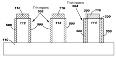
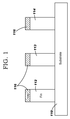
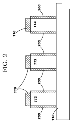
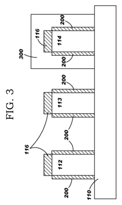
- A method of forming FinFET structures with multiple gate dielectric thicknesses by patterning fins, applying a first gate dielectric, protecting some fins with a mask, removing the dielectric from others, and adding additional dielectric layers to create different thicknesses, which also allows for multiple layers over some fins and single layers over others, enabling optimized performance and reliability.


Multiple dielectric finfet structure and method
PatentInactiveUS20070290250A1
Innovation
- A method of forming FinFETs with multiple gate dielectric thicknesses by patterning fins, applying a first gate dielectric, protecting some fins with a mask, removing it from others, and adding additional dielectric layers to achieve varying thicknesses, allowing for optimized performance and reliability across different regions.
Environmental Impact of Advanced Dielectric Materials
The environmental implications of advanced dielectric materials used in FinFET technology are becoming increasingly significant as semiconductor manufacturing scales up globally. High-k dielectric materials such as hafnium oxide (HfO2), zirconium oxide (ZrO2), and aluminum oxide (Al2O3) have replaced traditional silicon dioxide to enable continued device scaling, but their production, use, and disposal present unique environmental challenges.
Manufacturing these advanced dielectrics typically requires energy-intensive processes including atomic layer deposition (ALD) and chemical vapor deposition (CVD). These processes consume substantial electricity and often utilize precursor chemicals that may include rare earth elements or toxic compounds. The extraction of hafnium, for instance, generates significant mining waste and habitat disruption, while precursor chemicals like tetrakis(dimethylamino)hafnium (TDMAH) require careful handling and disposal protocols.
Water usage represents another critical environmental concern. The production of ultra-pure water necessary for semiconductor manufacturing consumes vast quantities of freshwater resources. A single semiconductor fabrication facility can use between 2-4 million gallons of water daily, with dielectric layer processing contributing significantly to this consumption. Efforts to optimize dielectric deposition processes must therefore consider water conservation strategies.
Chemical waste management presents ongoing challenges. Etching and cleaning processes associated with dielectric layer formation generate fluorinated compounds, acids, and solvents that require specialized treatment. While the semiconductor industry has made progress in chemical recovery and recycling systems, the increasing complexity of material stacks in advanced FinFETs complicates waste stream management.
Energy efficiency during device operation represents a positive environmental aspect of advanced dielectrics. By enabling lower operating voltages and reducing leakage current, high-k dielectrics contribute to decreased power consumption in electronic devices. This translates to extended battery life in mobile applications and reduced energy requirements in data centers, potentially offsetting some manufacturing-related environmental impacts.
End-of-life considerations for devices containing these materials remain problematic. The complex integration of multiple dielectric materials with different metals makes recycling challenging. Current electronic waste processing methods often fail to recover valuable materials from gate stacks, resulting in potential resource loss and environmental contamination.
Forward-looking environmental strategies include developing deposition techniques that minimize precursor waste, implementing closed-loop water recycling systems, and researching bio-derived or less toxic dielectric alternatives. Additionally, designing for disassembly and material recovery could improve the sustainability profile of FinFET technologies throughout their lifecycle.
Integration Challenges with Next-Gen Node Processes
The integration of optimized FinFET gate dielectrics with next-generation node processes presents significant challenges that require innovative solutions. As process nodes continue to shrink below 5nm, the complexity of integrating high-k dielectric materials with metal gates increases exponentially. The primary challenge lies in maintaining uniform dielectric thickness across the three-dimensional fin structure while ensuring minimal interface defects.
Material compatibility issues emerge when integrating new gate dielectric materials with existing process flows. Advanced high-k materials such as hafnium-based compounds must interface seamlessly with the channel material and metal gate electrodes. The thermal budget constraints of next-generation processes further complicate this integration, as post-deposition annealing temperatures must be carefully controlled to prevent crystallization or phase separation within the dielectric layer.
Atomic Layer Deposition (ALD) has become the preferred method for depositing gate dielectrics in advanced nodes, but achieving conformal coverage on high-aspect-ratio fins remains challenging. The precursor diffusion limitations and reaction kinetics can lead to thickness variations between the top and sidewalls of the fin structure, potentially compromising device performance and reliability.
Interface engineering represents another critical integration challenge. The quality of the interface between the silicon channel and the gate dielectric significantly impacts carrier mobility and threshold voltage stability. Next-generation processes must incorporate precise interface preparation steps, including advanced cleaning techniques and the formation of controlled interfacial layers.
The introduction of new channel materials such as SiGe, Ge, or III-V compounds in advanced nodes further complicates gate dielectric integration. These materials exhibit different surface chemistries and defect formation mechanisms compared to silicon, necessitating tailored dielectric deposition processes and interface treatments.
Metrology and characterization of ultra-thin gate dielectrics present additional challenges. As dielectric thickness approaches the sub-nanometer range, conventional measurement techniques become inadequate. Advanced analytical methods such as high-resolution TEM, XPS, and electrical characterization must be integrated into the process flow to ensure quality control.
The co-optimization of gate dielectrics with other process modules, including source/drain epitaxy, contact formation, and interconnect integration, requires a holistic approach. Changes in gate dielectric properties can impact subsequent process steps, necessitating comprehensive process integration strategies that consider the entire device fabrication flow.
Unlock deeper insights with Patsnap Eureka Quick Research — get a full tech report to explore trends and direct your research. Try now!
Generate Your Research Report Instantly with AI Agent
Supercharge your innovation with Patsnap Eureka AI Agent Platform!