PVDF in Transparent Electronics: Driving Innovation Forward
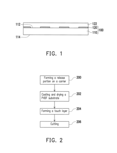
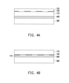
PVDF in Electronics: Background and Objectives
Polyvinylidene fluoride (PVDF) has emerged as a promising material in the field of transparent electronics, marking a significant milestone in the evolution of electronic devices. The journey of PVDF in this domain began with its discovery as a piezoelectric polymer in the 1960s, leading to its application in various sectors, including sensors and actuators. As the demand for flexible and transparent electronic components grew, researchers began exploring PVDF's potential in this arena.
The development of PVDF in transparent electronics is driven by the increasing need for devices that combine flexibility, transparency, and functionality. This trend aligns with the broader evolution of consumer electronics, wearable technology, and smart surfaces. PVDF's unique properties, such as its high dielectric constant, excellent mechanical flexibility, and optical transparency when properly processed, make it an ideal candidate for next-generation electronic applications.
The technical objectives for PVDF in transparent electronics are multifaceted. Primarily, researchers aim to enhance the material's transparency while maintaining its piezoelectric and ferroelectric properties. This involves optimizing the crystalline structure of PVDF and its copolymers to achieve a balance between optical clarity and electrical performance. Another key goal is to improve the material's compatibility with existing manufacturing processes, enabling seamless integration into current production lines.
Furthermore, the development of PVDF-based transparent electronics seeks to address the limitations of traditional materials like indium tin oxide (ITO), which, despite its widespread use, suffers from brittleness and scarcity of raw materials. PVDF offers a potential solution, promising durability, flexibility, and sustainability. Researchers are also focusing on enhancing the material's conductivity and charge carrier mobility to broaden its application in active electronic components.
The evolution of PVDF in transparent electronics is closely tied to advancements in nanotechnology and materials science. Recent years have seen significant progress in developing PVDF nanocomposites and thin films that exhibit improved transparency and electrical properties. These developments are paving the way for applications in touch screens, flexible displays, and transparent sensors, among others.
As we look to the future, the technical trajectory for PVDF in transparent electronics is aimed at achieving higher levels of integration and multifunctionality. This includes developing self-powered devices that leverage PVDF's piezoelectric properties, creating energy-harvesting transparent electronics, and exploring its potential in optoelectronic applications. The ultimate goal is to establish PVDF as a versatile platform material that can support a wide range of transparent electronic devices, from simple sensors to complex, multi-layered systems.
Market Demand Analysis for Transparent Electronics
The transparent electronics market has been experiencing significant growth in recent years, driven by the increasing demand for innovative display technologies and smart devices. This surge in market demand is primarily fueled by the consumer electronics sector, where transparent displays are becoming increasingly popular in smartphones, tablets, and wearable devices. The automotive industry is also showing a growing interest in transparent electronics for heads-up displays and smart windshields, contributing to the market's expansion.
The integration of PVDF (Polyvinylidene Fluoride) in transparent electronics is opening up new possibilities and addressing several key market needs. PVDF's unique properties, including its high transparency, flexibility, and piezoelectric characteristics, make it an attractive material for various applications in the transparent electronics field. This has led to a rising demand for PVDF-based components in the production of flexible displays, touch sensors, and energy harvesting devices.
In the consumer electronics segment, there is a growing trend towards foldable and rollable displays, where PVDF's flexibility and durability play a crucial role. Market research indicates that the foldable display market is expected to grow rapidly in the coming years, creating a substantial demand for materials like PVDF that can enable these innovative form factors.
The energy sector is another area driving the demand for PVDF in transparent electronics. With the increasing focus on renewable energy and energy efficiency, there is a growing interest in transparent solar cells and energy harvesting devices. PVDF's piezoelectric properties make it an excellent candidate for these applications, potentially leading to the development of windows that can generate electricity or self-powered electronic devices.
In the healthcare industry, there is a rising demand for wearable medical devices and smart healthcare solutions. PVDF's biocompatibility and flexibility make it suitable for developing transparent, skin-friendly sensors and monitoring devices. This aligns with the growing trend of personalized healthcare and remote patient monitoring, further expanding the market potential for PVDF in transparent electronics.
The automotive sector is also showing increased interest in transparent electronics, particularly for advanced driver assistance systems (ADAS) and in-vehicle infotainment. PVDF's ability to be integrated into transparent, flexible displays and touch interfaces is driving its adoption in next-generation automotive designs.
As the Internet of Things (IoT) continues to expand, there is a growing need for transparent, flexible sensors that can be seamlessly integrated into various environments. PVDF's properties make it well-suited for developing such sensors, potentially leading to new applications in smart homes, industrial automation, and environmental monitoring.
Current State and Challenges of PVDF in Transparent Electronics
Polyvinylidene fluoride (PVDF) has emerged as a promising material in the field of transparent electronics, offering unique properties that drive innovation forward. The current state of PVDF in this domain is characterized by significant advancements, yet it also faces several challenges that require further research and development.
PVDF's piezoelectric and ferroelectric properties have made it an attractive candidate for various transparent electronic applications. Its high transparency in the visible spectrum, coupled with its flexibility and durability, has led to its incorporation in touch sensors, displays, and energy harvesting devices. Recent studies have demonstrated the successful fabrication of PVDF-based transparent thin films with excellent optical and electrical properties, paving the way for next-generation flexible and wearable electronics.
One of the primary challenges in utilizing PVDF for transparent electronics lies in optimizing its crystalline structure. The β-phase of PVDF, which exhibits the strongest piezoelectric response, is crucial for many applications. However, achieving a high percentage of β-phase in transparent PVDF films without compromising optical clarity remains a significant hurdle. Researchers are exploring various techniques, such as mechanical stretching, electrical poling, and nanocomposite formation, to enhance β-phase content while maintaining transparency.
Another challenge is the integration of PVDF with other materials in multilayer transparent electronic devices. The compatibility of PVDF with common electrode materials and its adhesion to substrates are critical factors that affect device performance and longevity. Developing robust interfacial engineering techniques to ensure seamless integration of PVDF layers with other components is an ongoing area of research.
The scalability of PVDF-based transparent electronic devices presents another significant challenge. While laboratory-scale demonstrations have shown promising results, translating these achievements to large-scale, cost-effective manufacturing processes remains a hurdle. Issues such as uniformity in film thickness, consistency in electrical properties across large areas, and the development of high-throughput fabrication methods need to be addressed to enable commercial viability.
Environmental stability and long-term reliability of PVDF in transparent electronics are also areas of concern. The material's sensitivity to temperature and humidity fluctuations can affect its performance and lifespan in real-world applications. Developing strategies to enhance the environmental resilience of PVDF-based devices, such as encapsulation techniques or the incorporation of stabilizing additives, is crucial for their widespread adoption.
Despite these challenges, the current state of PVDF in transparent electronics is marked by rapid progress and innovation. Collaborative efforts between materials scientists, device engineers, and industry partners are driving advancements in PVDF technology. As research continues to address the existing challenges, PVDF is poised to play an increasingly important role in shaping the future of transparent and flexible electronic devices.
Existing PVDF Solutions for Transparent Electronics
01 Improving PVDF transparency through composition modification
The transparency of PVDF can be enhanced by modifying its composition. This may involve blending PVDF with other polymers or incorporating additives that improve light transmission. Such modifications can alter the crystalline structure of PVDF, reducing light scattering and increasing overall transparency.- Improving PVDF transparency through composition modification: Enhancing the transparency of PVDF can be achieved by modifying its composition. This may involve blending PVDF with other polymers or incorporating specific additives that improve light transmission. The modified composition aims to reduce light scattering within the material, resulting in increased transparency while maintaining PVDF's desirable properties.
- Processing techniques for transparent PVDF films: Various processing techniques can be employed to produce transparent PVDF films. These may include controlled crystallization, stretching, and thermal treatments. Optimizing processing parameters such as temperature, pressure, and cooling rates can significantly impact the optical properties of PVDF, leading to improved transparency.
- Nanocomposite approach for enhancing PVDF transparency: Incorporating nanoparticles or nanostructures into PVDF can enhance its transparency. This approach involves dispersing nanoscale materials throughout the PVDF matrix, which can reduce light scattering and improve overall optical clarity. The type, size, and distribution of nanoparticles play crucial roles in achieving the desired transparency.
- Surface treatment methods for transparent PVDF: Surface treatments can be applied to PVDF to enhance its transparency. These treatments may include plasma processing, chemical etching, or coating applications. By modifying the surface characteristics of PVDF, light reflection can be reduced, and transmission can be improved, resulting in increased transparency.
- Optical additives for PVDF transparency enhancement: Specific optical additives can be incorporated into PVDF to improve its transparency. These additives may include light-transmitting particles, clarifying agents, or specialized dyes. The careful selection and integration of these additives can help reduce haze, increase light transmission, and enhance the overall optical clarity of PVDF materials.
02 Processing techniques for transparent PVDF films
Various processing techniques can be employed to produce transparent PVDF films. These may include controlled cooling rates during film formation, stretching processes, or specific extrusion methods. These techniques aim to manipulate the polymer's molecular orientation and crystallinity, resulting in improved optical properties.Expand Specific Solutions03 Surface treatment methods for enhancing PVDF transparency
Surface treatments can be applied to PVDF to improve its transparency. These may include plasma treatment, chemical etching, or the application of anti-reflective coatings. Such treatments can modify the surface properties of PVDF, reducing light reflection and increasing light transmission through the material.Expand Specific Solutions04 Nanocomposite formulations for transparent PVDF
Incorporating nanoparticles or nanostructures into PVDF can enhance its transparency. These nanocomposites may utilize materials such as silica, titanium dioxide, or carbon nanotubes. The nanoparticles can help to reduce light scattering within the polymer matrix, leading to improved optical clarity.Expand Specific Solutions05 Optical property enhancement through copolymerization
Copolymerization of PVDF with other monomers can lead to improved transparency. This approach involves introducing specific co-monomers during the polymerization process, which can alter the polymer's structure and properties. The resulting copolymers may exhibit enhanced optical characteristics compared to pure PVDF.Expand Specific Solutions
Key Players in PVDF and Transparent Electronics Industry
The PVDF in transparent electronics market is in a growth phase, driven by increasing demand for flexible and transparent displays. The market size is expanding rapidly, with major players like Samsung SDI, LG Display, and BOE Technology Group leading innovation. Technological maturity varies, with established companies like Arkema and Merck Patent GmbH focusing on material development, while emerging players like Ubiquitous Energy explore novel applications. Research institutions such as Industrial Technology Research Institute and Electronics & Telecommunications Research Institute contribute to advancing PVDF technology. The competitive landscape is dynamic, with both large corporations and specialized firms vying for market share in this promising field.
Samsung SDI Co., Ltd.
BOE Technology Group Co., Ltd.
Core Innovations in PVDF for Transparent Devices
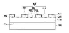
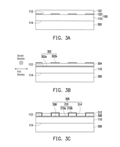
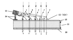
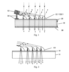
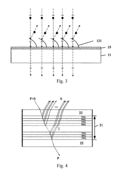
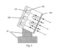
- A touch panel comprising a PVDF substrate with an inorganic nano-modified material dispersion, where the touch electrode structure is disposed on at least one surface of the PVDF substrate, and optionally a passivation layer or functional film is used to enhance optical properties and tactile feedback.
- A transparent display device design featuring a display panel with a polarizer on one side and an array of polarization light splitting sheets on the other, where the polarization light sheets are inclined at a specific angle to reflect polarized light from a source and transmit ambient light, enhancing light transmittance and transparency.
Environmental Impact of PVDF in Electronics
The environmental impact of PVDF (Polyvinylidene fluoride) in electronics, particularly in transparent electronic applications, is a critical consideration as the technology advances. PVDF's unique properties, including its piezoelectric and ferroelectric characteristics, make it an attractive material for various electronic components. However, its widespread use also raises concerns about its ecological footprint.
PVDF production involves the polymerization of vinylidene fluoride, a process that requires significant energy input and potentially harmful chemicals. The manufacturing process may release fluorinated compounds, which can persist in the environment and potentially impact ecosystems. Additionally, the use of solvents in PVDF processing can contribute to air and water pollution if not properly managed.
On the positive side, PVDF's durability and resistance to degradation can lead to longer-lasting electronic devices, potentially reducing electronic waste. Its ability to function efficiently in various environmental conditions may also contribute to the development of more robust and energy-efficient electronic systems, indirectly benefiting the environment through reduced energy consumption.
The recyclability of PVDF in electronic applications is an area of ongoing research and development. While PVDF itself is recyclable, its integration into complex electronic devices can make the recycling process challenging. Efforts are being made to develop more effective recycling methods for PVDF-containing electronics, which could significantly reduce the material's end-of-life environmental impact.
In transparent electronics, PVDF's potential to replace other materials with higher environmental impacts is noteworthy. For instance, if PVDF-based transparent conductors can replace indium tin oxide (ITO), which relies on the scarce element indium, it could lead to more sustainable production of transparent electronic devices.
The use of PVDF in flexible and wearable electronics presents both opportunities and challenges from an environmental perspective. While these applications may lead to more efficient and longer-lasting devices, the integration of PVDF with other materials in these complex systems may complicate end-of-life disposal and recycling processes.
As research in PVDF-based transparent electronics progresses, there is a growing focus on developing more environmentally friendly synthesis methods and exploring bio-based alternatives. These efforts aim to reduce the environmental footprint of PVDF production and use while maintaining its beneficial properties for electronic applications.
Scalability and Manufacturing Considerations
The scalability and manufacturing considerations for PVDF in transparent electronics are crucial factors in driving innovation forward. As the demand for flexible and transparent electronic devices continues to grow, the ability to produce PVDF-based components at scale becomes increasingly important.
One of the primary challenges in scaling up PVDF production for transparent electronics lies in maintaining consistent material properties across large-scale manufacturing processes. The piezoelectric and ferroelectric properties of PVDF, which are essential for its application in transparent electronics, are highly dependent on the polymer's crystalline structure. Ensuring uniformity in crystal formation and orientation during mass production requires precise control over processing parameters such as temperature, pressure, and cooling rates.
Solution processing techniques, such as spin-coating and blade-coating, have shown promise for large-area fabrication of PVDF thin films. These methods offer the advantage of being compatible with roll-to-roll manufacturing processes, which are ideal for high-throughput production of flexible electronic devices. However, optimizing these techniques for consistent film thickness and quality across large areas remains an ongoing challenge.
Another critical aspect of scalability is the development of efficient electrode deposition methods that are compatible with PVDF's unique surface properties. Transparent conductive electrodes, such as indium tin oxide (ITO) or graphene, must be deposited without compromising the PVDF film's transparency or piezoelectric performance. Advances in low-temperature deposition techniques and novel electrode materials are essential for overcoming this hurdle.
The integration of PVDF into complex device architectures presents additional manufacturing challenges. As transparent electronics often involve multilayer structures, the development of reliable lamination and bonding processes that maintain PVDF's functional properties is crucial. This includes addressing issues related to thermal stability and chemical compatibility with other materials used in the device stack.
Environmental considerations also play a significant role in scaling up PVDF production for transparent electronics. The use of environmentally friendly solvents and processing methods is becoming increasingly important, driving research into green manufacturing techniques that minimize the use of harmful chemicals while maintaining product quality and performance.
As the field progresses, the development of in-line quality control and characterization methods will be essential for ensuring consistent performance of PVDF-based transparent electronic components. This may involve the implementation of advanced spectroscopic and imaging techniques capable of rapidly assessing film quality, crystallinity, and functional properties during the manufacturing process.