

Receiver PV Cell Selection: GaAs vs. Si vs. Multi-Junction Options
AUG 28, 20259 MIN READ
Generate Your Research Report Instantly with AI Agent
PatSnap Eureka helps you evaluate technical feasibility & market potential.
PV Receiver Technology Background and Objectives
Photovoltaic (PV) receiver technology has evolved significantly over the past decades, transitioning from simple silicon-based cells to advanced multi-junction architectures. The journey began in the 1950s with the development of silicon PV cells at Bell Laboratories, achieving initial efficiencies of around 6%. By the 1970s, gallium arsenide (GaAs) emerged as a promising alternative, particularly for space applications due to its higher efficiency and radiation resistance.
The fundamental objective of PV receiver technology is to maximize the conversion of solar energy into electrical power while minimizing costs and ensuring reliability. This balance between performance and economic viability continues to drive innovation in the field. Different materials offer distinct advantages: silicon provides cost-effectiveness and manufacturing scalability, GaAs delivers superior efficiency and performance under concentrated light, while multi-junction designs capture broader portions of the solar spectrum.
Current technological trajectories indicate a growing interest in specialized applications where the unique properties of each cell type can be leveraged optimally. For concentrated photovoltaic (CPV) systems, which focus sunlight onto small receiver areas, the selection of appropriate PV cell technology becomes particularly critical due to the intense operating conditions and performance requirements.
The global push toward renewable energy has accelerated research in PV receiver technology, with significant investments from both public and private sectors. Research institutions and corporations worldwide are exploring novel materials, manufacturing techniques, and cell architectures to overcome existing limitations. The U.S. Department of Energy's Sunshot Initiative, European Union's Horizon programs, and similar efforts in China and Japan have established ambitious targets for efficiency improvements and cost reductions.
Technical objectives in this field include achieving theoretical efficiency limits, enhancing thermal stability under concentrated light conditions, improving manufacturing yields, and extending operational lifetimes. For GaAs cells, researchers aim to reduce production costs while maintaining their superior efficiency. Silicon technology focuses on pushing efficiency boundaries while preserving its cost advantage. Multi-junction approaches seek to optimize layer combinations and interfaces to maximize spectrum utilization.
The selection between GaAs, Si, and multi-junction options represents a critical decision point for system designers, with implications for overall system performance, reliability, and economic viability. This decision must consider not only current technological capabilities but also anticipated advancements and scaling potential. The optimal choice varies significantly based on specific application requirements, geographical deployment location, and project economics.
As the renewable energy landscape evolves, PV receiver technology continues to advance toward higher efficiencies, lower costs, and broader applicability, making the selection process increasingly nuanced and consequential for system designers and energy providers.
Market Analysis for Advanced PV Cell Applications
The global market for advanced photovoltaic (PV) cell technologies is experiencing significant growth, driven by increasing demand for renewable energy solutions and improved energy conversion efficiency. The market for GaAs (Gallium Arsenide), Silicon (Si), and Multi-Junction PV cells collectively reached approximately $15 billion in 2022, with projections indicating growth to $25 billion by 2027, representing a compound annual growth rate of 10.8%.
Silicon-based PV cells continue to dominate the market with over 90% market share due to their cost-effectiveness and established manufacturing infrastructure. However, high-efficiency alternatives are gaining traction in specialized applications. The GaAs PV cell market segment, valued at $1.2 billion in 2022, is growing at 12% annually, primarily driven by space applications and concentrated photovoltaic systems where efficiency is paramount.
Multi-junction PV cells, though representing a smaller market segment at $800 million, are experiencing the fastest growth rate at 15% annually. This growth is fueled by their superior efficiency in specialized applications such as satellites, space exploration, and high-concentration solar systems.
Regional analysis reveals that North America leads in advanced PV cell research and deployment, particularly in aerospace and defense applications. Asia-Pacific, led by China and Japan, dominates manufacturing capacity for all PV technologies, while Europe focuses on high-efficiency applications and innovative integration solutions.
Market segmentation by application shows distinct preferences: aerospace and satellite applications favor GaAs and multi-junction cells due to their high efficiency and radiation resistance. Concentrated photovoltaic (CPV) systems primarily utilize multi-junction cells to maximize energy harvest from concentrated sunlight. Consumer electronics increasingly incorporate GaAs cells for portable power applications.
Key market drivers include efficiency requirements for space-constrained applications, declining manufacturing costs through improved processes, and increasing demand for renewable energy in specialized sectors. The premium market for high-efficiency cells is expanding as efficiency advantages increasingly outweigh cost considerations in certain applications.
Challenges facing market growth include high production costs compared to conventional silicon cells, limited manufacturing scale for advanced technologies, and competition from continuously improving silicon technology. The cost-per-watt metric remains a significant barrier to wider adoption outside of specialized applications where performance requirements justify premium pricing.
Current State and Challenges in PV Cell Technologies
Photovoltaic (PV) cell technology has evolved significantly over the past decades, with various materials and designs competing for dominance in different application scenarios. Currently, three main PV cell technologies stand at the forefront of receiver applications: Silicon (Si), Gallium Arsenide (GaAs), and Multi-Junction cells. Each presents distinct advantages and limitations that shape their market adoption and technological trajectory.
Silicon-based PV cells continue to dominate the global market, accounting for approximately 95% of commercial installations. This dominance stems from silicon's abundance, established manufacturing infrastructure, and relatively low production costs. Modern silicon cells achieve efficiencies of 18-22% in commercial applications, with laboratory specimens reaching up to 26.7%. However, silicon cells face fundamental limitations including moderate bandgap properties that restrict theoretical efficiency to around 29% under standard conditions.
GaAs technology represents a significant advancement in single-junction cell performance, demonstrating superior efficiency rates of 27-29% in production settings and exceeding 30% in laboratory environments. These cells exhibit excellent performance under concentrated light and maintain higher efficiency at elevated temperatures compared to silicon alternatives. Despite these advantages, GaAs cells face substantial challenges in widespread adoption due to manufacturing complexity, gallium scarcity, and production costs approximately 5-10 times higher than silicon counterparts.
Multi-Junction cells, incorporating multiple semiconductor layers with varying bandgaps, currently hold the efficiency record among PV technologies. Commercial triple-junction cells routinely achieve 30-38% efficiency, while advanced research prototypes have demonstrated over 47% efficiency under concentrated sunlight. These cells excel in space applications and concentrated photovoltaic (CPV) systems where space constraints justify their premium cost.
The geographical distribution of these technologies reveals interesting patterns. Silicon manufacturing has concentrated in China, which controls over 70% of global production capacity. GaAs development remains centered in advanced economies including the United States, Germany, and Japan. Multi-Junction research clusters around specialized institutions in the United States, Europe, and increasingly in China and South Korea.
Key technical challenges persist across all three technologies. Silicon cells struggle with light-induced degradation and efficiency plateaus approaching theoretical limits. GaAs faces critical materials supply constraints and manufacturing scalability issues. Multi-Junction cells continue to battle interface defects, thermal management complexities, and prohibitive production costs that limit their application to specialized markets.
Environmental considerations also present challenges, particularly regarding the toxicity of materials used in GaAs and certain Multi-Junction cells, along with end-of-life recycling complexities. Regulatory frameworks worldwide are increasingly addressing these concerns, potentially influencing future technology adoption patterns.
Comparative Analysis of GaAs, Si, and Multi-Junction Solutions
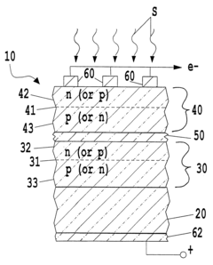
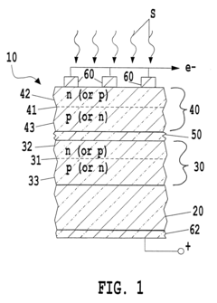
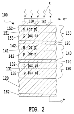
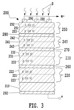
01 Multi-junction solar cell efficiency improvements
Multi-junction solar cells achieve higher efficiency by stacking multiple semiconductor layers that absorb different wavelengths of light. These cells typically use combinations of materials like GaAs, InGaP, and Ge to capture a broader spectrum of sunlight. Advanced designs incorporate tunnel junctions between subcells to facilitate current flow, while optimized bandgap engineering ensures maximum energy conversion. Recent innovations include improved lattice matching techniques and novel material combinations that push efficiency beyond 40%.- Multi-junction solar cell efficiency improvements: Multi-junction solar cells achieve higher efficiency by stacking multiple semiconductor layers that absorb different wavelengths of light. These cells typically use combinations of materials like GaAs, InGaP, and Ge to capture a broader spectrum of sunlight. Advanced designs incorporate tunnel junctions between subcells to facilitate current flow, while optimized bandgap engineering ensures maximum energy conversion. Recent innovations include improved lattice matching techniques and novel material combinations that push efficiency beyond 40%.
- Silicon-based PV cell efficiency enhancements: Silicon-based photovoltaic cells remain the most widely used technology due to material abundance and established manufacturing processes. Efficiency improvements focus on reducing recombination losses through advanced surface passivation techniques, implementing selective emitter structures, and optimizing contact designs. Innovations include heterojunction architectures, back-contact configurations, and light-trapping textures that minimize reflection losses. These advancements have pushed commercial Si cell efficiencies toward 25%, approaching the theoretical limit for single-junction silicon devices.
- GaAs solar cell technology advancements: Gallium arsenide solar cells offer superior efficiency compared to silicon due to their direct bandgap and excellent electron mobility properties. Recent advancements include epitaxial lift-off techniques that allow substrate reuse, reducing manufacturing costs while maintaining high performance. Innovations in growth methods have minimized defect densities, while novel device architectures optimize carrier collection. These cells demonstrate exceptional performance under concentrated sunlight and are increasingly used in space applications where high efficiency-to-weight ratio is critical.
- Novel materials and structures for efficiency enhancement: Research into novel materials and structures has yielded significant efficiency improvements in photovoltaic cells. Approaches include incorporating quantum dots and nanowires to enhance light absorption, implementing intermediate band structures to capture sub-bandgap photons, and developing perovskite-silicon tandem cells. Advanced light management techniques using photonic structures and plasmonic effects further boost performance. These innovations address fundamental efficiency limitations of conventional designs and offer pathways toward exceeding the Shockley-Queisser limit for single-junction devices.
- Manufacturing and integration techniques for high-efficiency PV cells: Advanced manufacturing and integration techniques play a crucial role in translating theoretical efficiency gains into commercially viable photovoltaic products. Innovations include precision deposition methods for uniform thin films, improved metallization techniques that reduce shadowing losses, and automated assembly processes for multi-junction stacks. Novel interconnection approaches minimize resistive losses in module integration, while specialized encapsulation methods enhance durability without compromising optical performance. These manufacturing advances help bridge the gap between laboratory records and mass-produced solar cell efficiencies.
02 Silicon-based PV cell efficiency enhancements
Silicon remains the dominant material for commercial photovoltaics due to its abundance and established manufacturing processes. Efficiency improvements focus on reducing recombination losses through advanced surface passivation techniques, implementing selective emitter structures, and optimizing contact designs. Heterojunction technologies combining crystalline and amorphous silicon layers have demonstrated increased efficiency. Other approaches include light trapping structures, anti-reflection coatings, and back-contact designs that minimize shading losses on the front surface.Expand Specific Solutions03 GaAs solar cell technology advancements
Gallium arsenide solar cells offer superior efficiency compared to silicon due to their direct bandgap and excellent electron mobility. Recent advancements include epitaxial lift-off techniques that allow substrate reuse, reducing manufacturing costs. Innovations in growth methods have minimized defects and improved material quality. Novel device architectures incorporating quantum wells or quantum dots enable bandgap engineering for optimized light absorption. Thin-film GaAs approaches have demonstrated high efficiency while using significantly less material than conventional designs.Expand Specific Solutions04 Novel materials and structures for high-efficiency PV cells
Research into novel materials and structures has expanded the efficiency potential of photovoltaic cells. Perovskite materials offer promising efficiency with lower manufacturing costs. Quantum structures like wells, dots, and wires enable precise bandgap tuning. Nanowire architectures provide enhanced light trapping and carrier collection. Two-dimensional materials show unique optoelectronic properties beneficial for solar applications. Hybrid approaches combining different material systems leverage the advantages of each to achieve higher overall conversion efficiency.Expand Specific Solutions05 Concentration photovoltaic systems for efficiency enhancement
Concentration photovoltaic (CPV) systems use optical elements to focus sunlight onto small, high-efficiency solar cells, significantly increasing power output. These systems typically employ multi-junction cells optimized for concentrated light conditions, achieving efficiencies exceeding 40%. Advanced thermal management techniques prevent efficiency degradation at high concentration ratios. Dual-axis tracking ensures maximum light capture throughout the day. Innovations in fresnel lenses, reflective optics, and spectral splitting technologies further enhance system performance while reducing material costs.Expand Specific Solutions
Key Industry Players in PV Cell Manufacturing
The photovoltaic receiver cell technology landscape is currently in a mature growth phase with increasing market diversification. The global market for PV receiver cells is expanding rapidly, projected to reach approximately $25-30 billion by 2025, driven by space applications, concentrated photovoltaics, and renewable energy initiatives. GaAs technology offers superior efficiency but at higher costs, championed by AZUR Space and Alta Devices. Silicon dominates commercial applications due to cost-effectiveness, with TSMC and Sharp leading manufacturing innovation. Multi-junction cells represent the cutting edge with efficiency exceeding 45%, developed by Boeing, AZUR Space, and research institutions like Australian National University. The competitive landscape shows regional specialization with European and American companies focusing on high-efficiency solutions while Asian manufacturers like Huawei and Sanan Optoelectronics drive cost optimization and mass production capabilities.
AZUR Space Solar Power GmbH
Technical Solution: AZUR Space has developed advanced multi-junction solar cells specifically designed for concentrated photovoltaic (CPV) applications, achieving conversion efficiencies exceeding 40% under concentrated sunlight. Their triple-junction GaInP/GaInAs/Ge cells utilize precise epitaxial growth techniques to create optimized bandgap combinations that capture different portions of the solar spectrum. The company has pioneered germanium substrate technology for III-V semiconductor growth, enabling high-quality crystal structures with minimal defects. AZUR's cells incorporate sophisticated anti-reflective coatings and front metal grid designs to minimize optical losses while maintaining excellent electrical performance. Their manufacturing process includes rigorous quality control measures with specialized testing under various concentration ratios and temperature conditions to ensure reliability in real-world applications.
Strengths: Industry-leading efficiency rates in multi-junction cells; extensive space heritage providing proven reliability data; advanced manufacturing capabilities for high-volume production. Weaknesses: Higher production costs compared to silicon alternatives; requires specialized mounting and tracking systems for terrestrial applications; more complex manufacturing process increasing potential failure points.
Alta Devices, Inc.
Technical Solution: Alta Devices has pioneered an innovative thin-film GaAs technology using an epitaxial lift-off process that allows for the reuse of expensive GaAs substrates, significantly reducing manufacturing costs. Their single-junction GaAs cells have achieved record efficiencies of over 28% for single-junction designs under one-sun conditions, the highest among all single-junction technologies. The company's proprietary manufacturing approach creates extremely thin (less than 1 micron) and lightweight flexible solar cells that maintain high performance even in low-light and high-temperature conditions. Alta's technology incorporates advanced photon recycling techniques where photons that aren't initially absorbed are reflected back into the cell, increasing overall quantum efficiency. Their cells feature specialized surface passivation layers that minimize recombination losses at interfaces, contributing to their exceptional voltage output characteristics.
Strengths: Highest single-junction efficiency commercially available; extremely lightweight and flexible form factor enabling new applications; superior performance in low-light and high-temperature conditions. Weaknesses: Higher production costs than silicon despite substrate reuse innovations; limited production scale compared to silicon manufacturers; company has faced financial challenges affecting market stability.
Critical Patents and Research in Advanced PV Cell Design
High efficiency multijunction photovoltaic cells
PatentInactiveUS20210126148A1
Innovation
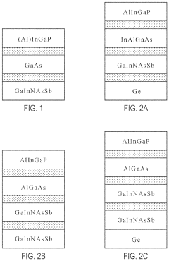
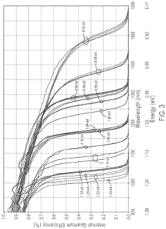
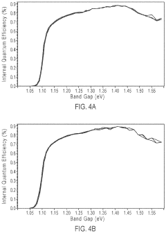
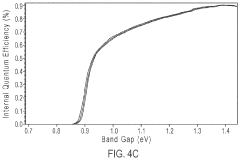
- The development of multijunction photovoltaic cells with four, five, or more subcells using GaInNAsSb semiconductor material, where the subcells are substantially lattice-matched to each other and a substrate, allowing for higher internal quantum efficiencies and reduced series resistance losses by tailoring the band gap and lattice constant of GaInNAsSb subcells.
Multi-junction, monolithic solar cell using low-band-gap materials lattice matched to GaAs or Ge
PatentInactiveUS6281426B1
Innovation
- The development of a multi-junction, monolithic solar cell device with semiconductor cells lattice-matched to GaAs or Ge substrates, featuring a series connection of junctions with carefully selected band gaps and materials like GaInAsN, GaAsGe, GaInAsP, and Ge to optimize energy conversion, including the use of tunnel junctions for efficient photocurrent flow and incremental energy absorption.
Environmental Impact and Sustainability Considerations
The environmental impact of photovoltaic (PV) cell technologies represents a critical consideration in the selection process for receiver applications. Silicon-based cells, while offering the advantage of utilizing abundant raw materials, require significant energy during manufacturing, resulting in a substantial carbon footprint. The production process involves energy-intensive purification of silicon, which generates considerable greenhouse gas emissions. However, silicon cells generally have a lower toxic material profile compared to other options, and established recycling infrastructure exists for end-of-life management.
GaAs (Gallium Arsenide) cells present a more complex environmental profile. The manufacturing process requires less energy than silicon, potentially reducing production-phase emissions. However, the extraction and processing of gallium and particularly arsenic involve significant environmental concerns. Arsenic is highly toxic, necessitating stringent safety protocols during production and raising serious end-of-life disposal challenges. The limited availability of gallium also raises resource depletion concerns, though its recovery from production waste is increasingly practiced.
Multi-junction cells combine the environmental considerations of their constituent materials, often incorporating rare elements like germanium, indium, and gallium. Their production complexity results in higher embodied energy, but this may be offset by their superior efficiency in application. The higher efficiency translates to smaller required cell area for equivalent power output, potentially reducing material usage and associated environmental impacts over the system lifetime.
Life cycle assessment (LCA) data indicates that energy payback periods vary significantly: approximately 1-2 years for silicon, 1-1.5 years for GaAs, and potentially shorter periods for multi-junction cells in high-concentration applications. These figures are continually improving as manufacturing processes become more efficient and material utilization rates increase.
Water consumption represents another important sustainability metric, with GaAs and multi-junction manufacturing typically requiring more ultrapure water than silicon cell production. This consideration becomes particularly relevant in water-stressed regions where manufacturing facilities might be located.
Circular economy principles are increasingly being applied to PV technologies, with research focusing on design-for-recycling approaches. Silicon cells currently have the most mature recycling pathways, while GaAs and multi-junction technologies present greater challenges due to their complex material compositions and the presence of potentially hazardous elements.
Cost-Performance Analysis Across PV Cell Technologies
When evaluating photovoltaic (PV) cell technologies for receiver applications, cost-performance analysis reveals significant variations across Silicon (Si), Gallium Arsenide (GaAs), and Multi-Junction options. Silicon cells dominate the commercial market due to their cost advantage, typically priced at $0.20-0.30 per watt, compared to GaAs at $5-10 per watt and multi-junction cells exceeding $20 per watt. This substantial cost differential stems from manufacturing scale economies, material availability, and production complexity.
Efficiency metrics demonstrate an inverse relationship with cost factors. Silicon cells generally achieve 18-22% efficiency in commercial applications, while GaAs cells deliver 27-32% efficiency. Multi-junction cells substantially outperform both with 38-47% efficiency rates, particularly in concentrated photovoltaic systems. This efficiency advantage becomes crucial in space-constrained applications or where system-level costs outweigh cell costs.
Lifetime performance considerations further complicate the analysis. Silicon cells typically degrade at 0.5-1% annually, while GaAs demonstrates superior degradation resistance at 0.3-0.5% annually. Multi-junction cells, despite their complexity, often match GaAs in degradation resilience, maintaining higher absolute efficiency even after years of operation.
Temperature coefficient analysis reveals GaAs cells lose approximately 0.1-0.2% efficiency per degree Celsius above standard testing conditions, compared to silicon's 0.4-0.5% loss. This thermal stability provides significant advantages in high-temperature environments like concentrated solar applications, where operating temperatures frequently exceed 70°C.
Return on investment calculations must incorporate these performance differentials against initial capital expenditure. For terrestrial applications with space constraints, GaAs cells reach financial breakeven 30-40% faster than silicon despite higher upfront costs. Multi-junction cells, while requiring substantial initial investment, demonstrate compelling economics in high-DNI (Direct Normal Irradiance) regions when paired with concentration systems exceeding 500x.
Manufacturing scalability presents another critical dimension. Silicon benefits from decades of semiconductor industry development and gigawatt-scale production capacity. GaAs manufacturing remains limited to specialized facilities with production volumes orders of magnitude smaller. Multi-junction cell production is further constrained, primarily serving space and military applications where performance supersedes cost considerations.
Unlock deeper insights with PatSnap Eureka Quick Research — get a full tech report to explore trends and direct your research. Try now!
Generate Your Research Report Instantly with AI Agent
Supercharge your innovation with PatSnap Eureka AI Agent Platform!