

UCIe Multi-Die Memory: Bandwidth Density, Access Efficiency And Contention
SEP 22, 20259 MIN READ
Generate Your Research Report Instantly with AI Agent
PatSnap Eureka helps you evaluate technical feasibility & market potential.
UCIe Multi-Die Memory Evolution and Objectives
The Universal Chiplet Interconnect Express (UCIe) represents a significant evolution in memory architecture, transitioning from traditional monolithic designs to disaggregated multi-die configurations. This paradigm shift has been driven by the increasing demands for higher memory bandwidth, improved energy efficiency, and reduced latency in data-intensive applications such as artificial intelligence, high-performance computing, and large-scale data analytics.
The historical trajectory of memory technology has been characterized by continuous improvements in density and performance, from DDR to HBM and now to UCIe-based multi-die memory solutions. The limitations of traditional memory architectures became increasingly apparent as computational workloads grew more complex and data-intensive, necessitating a fundamental rethinking of memory system design.
UCIe multi-die memory technology emerged as a response to these challenges, offering a modular approach that enables the integration of heterogeneous memory dies within a single package. This approach leverages advanced packaging technologies such as 2.5D and 3D integration to achieve unprecedented levels of memory bandwidth density while maintaining reasonable power consumption profiles.
The primary objectives of UCIe multi-die memory development include achieving bandwidth densities exceeding 8 TB/s per package, reducing access latencies to sub-10 nanoseconds, and improving energy efficiency to less than 1 pJ/bit. These ambitious targets are essential for supporting next-generation computational workloads that require massive parallel data access and processing capabilities.
Another critical objective is to establish a standardized interconnect framework that enables interoperability between chiplets from different vendors, fostering an open ecosystem that accelerates innovation and reduces development costs. This standardization effort aims to create a unified approach to addressing the memory wall problem that has long constrained system performance.
The evolution of UCIe multi-die memory also seeks to address the growing concerns around memory contention in multi-core and multi-processor systems. By providing more sophisticated memory partitioning and access mechanisms, UCIe technology aims to minimize contention-related performance bottlenecks that plague current memory architectures.
Looking forward, the roadmap for UCIe multi-die memory includes further refinements in die-to-die communication protocols, enhanced thermal management techniques, and more sophisticated memory controllers capable of dynamically optimizing access patterns based on workload characteristics. These advancements will be crucial for meeting the exponentially growing memory demands of emerging applications in artificial intelligence, quantum computing simulation, and real-time analytics.
Market Demand Analysis for High-Bandwidth Memory Solutions
The high-bandwidth memory (HBM) market is experiencing unprecedented growth driven by the explosive demand for data-intensive applications across multiple sectors. Current market analysis indicates that the global HBM market is projected to grow at a CAGR of 23.5% through 2028, reaching a market value of over $14 billion. This remarkable growth trajectory is primarily fueled by the increasing adoption of artificial intelligence, machine learning, and high-performance computing applications that require massive parallel processing capabilities.
The emergence of UCIe (Universal Chiplet Interconnect Express) Multi-Die Memory architectures represents a direct response to these escalating market demands. Data centers and cloud service providers are particularly driving this demand, as they face mounting pressure to process exponentially growing datasets while maintaining energy efficiency. These providers require memory solutions that can deliver bandwidth densities exceeding 2 TB/s per package while maintaining reasonable power envelopes.
Enterprise customers are increasingly prioritizing memory solutions that offer not just raw bandwidth, but also improved access efficiency. Market research indicates that approximately 65% of enterprise customers cite memory access latency as a critical bottleneck in their high-performance computing applications. The ability of UCIe Multi-Die Memory to potentially reduce memory access contention through advanced scheduling algorithms and improved die-to-die interconnects directly addresses this market pain point.
The automotive and edge computing sectors represent emerging market opportunities for high-bandwidth memory solutions. As autonomous driving systems evolve, they require real-time processing of sensor data with stringent latency requirements. Market forecasts suggest that automotive applications for high-bandwidth memory will grow at 31% annually through 2027, outpacing the broader market.
Consumer electronics manufacturers are also showing increased interest in high-bandwidth memory solutions as mobile devices incorporate more AI capabilities. This segment values the power efficiency aspects of UCIe Multi-Die Memory, with market surveys indicating that 78% of smartphone manufacturers plan to incorporate some form of high-bandwidth memory in their flagship devices within the next three product cycles.
From a geographical perspective, North America currently leads the market demand for high-bandwidth memory solutions, accounting for approximately 42% of global consumption. However, the Asia-Pacific region is expected to show the fastest growth rate at 27% annually, driven by the rapid expansion of data centers and AI research initiatives in China, South Korea, and Taiwan.
Current UCIe Multi-Die Memory Challenges
UCIe Multi-Die Memory technology faces several significant challenges that impede its full potential in modern computing systems. The bandwidth density limitations represent a primary concern, as current implementations struggle to achieve the theoretical maximum data transfer rates across die-to-die interfaces. This limitation stems from physical constraints in interconnect design, signal integrity issues at high frequencies, and thermal considerations that restrict operational parameters.
Access efficiency presents another critical challenge, with memory access latencies varying significantly depending on the physical location of memory resources relative to compute elements. This non-uniform memory access (NUMA) effect becomes more pronounced in complex multi-die configurations, creating performance inconsistencies that are difficult to predict and optimize for in software applications. Current memory controllers lack sophisticated mechanisms to effectively manage these variable latencies.
Memory contention issues arise when multiple processing elements simultaneously attempt to access shared memory resources across die boundaries. The arbitration mechanisms currently employed often introduce additional latency and can lead to performance bottlenecks, particularly under heavy workloads with irregular access patterns. This contention problem scales non-linearly with the number of dies and processing elements in the system.
Power management represents a substantial challenge for UCIe Multi-Die Memory systems. The energy required for data movement across die boundaries can account for a significant portion of the total system power budget. Current solutions lack granular power control mechanisms that can dynamically adjust power allocation based on workload characteristics and thermal conditions.
Reliability concerns also persist, particularly regarding signal integrity across die interfaces. As data rates increase, maintaining error-free transmission becomes increasingly difficult, necessitating more complex error correction mechanisms that introduce additional overhead and latency. The long-term reliability of high-frequency die-to-die interconnects under various environmental conditions remains inadequately characterized.
Manufacturing and testing complexities further complicate UCIe Multi-Die Memory implementation. The yield challenges associated with producing multiple high-quality dies and integrating them with precise alignment requirements increase production costs. Current testing methodologies are insufficient for comprehensively validating complex multi-die memory subsystems, potentially allowing defects to escape detection.
Standardization efforts, while progressing, have not yet fully matured to enable seamless interoperability between components from different vendors. This fragmentation in the ecosystem limits adoption and increases integration costs for system designers seeking to leverage UCIe Multi-Die Memory technology.
Current Architectural Solutions for Bandwidth Optimization
01 UCIe Multi-Die Memory Architecture and Bandwidth Optimization
Universal Chiplet Interconnect Express (UCIe) technology enables high-bandwidth, low-latency connections between multiple memory dies in advanced computing systems. This architecture optimizes memory bandwidth density by facilitating efficient data transfer between chiplets, reducing interconnect bottlenecks, and supporting parallel memory access across multiple dies. The implementation includes specialized routing mechanisms and interface protocols that maintain signal integrity while maximizing data throughput.- UCIe architecture for multi-die memory systems: Universal Chiplet Interconnect Express (UCIe) architecture enables high-bandwidth, low-latency connections between multiple memory dies in advanced computing systems. This architecture supports efficient data transfer between chiplets, allowing for increased memory bandwidth density through optimized die-to-die interfaces. The implementation includes standardized protocols that facilitate seamless integration of heterogeneous memory components while maintaining system coherence.
- Memory bandwidth optimization techniques: Various techniques are employed to optimize memory bandwidth in multi-die systems, including parallel access mechanisms, advanced caching algorithms, and memory interleaving. These approaches distribute memory accesses across multiple channels to increase effective bandwidth density. By implementing sophisticated memory controllers that can dynamically allocate resources based on workload characteristics, the system can achieve higher throughput while minimizing latency, particularly important for data-intensive applications.
- Access efficiency improvements for multi-die memory: Memory access efficiency in UCIe-based systems is enhanced through specialized scheduling algorithms, predictive prefetching, and optimized memory mapping strategies. These techniques reduce access latency and improve overall system performance by minimizing idle cycles and maximizing data throughput. Advanced memory controllers implement intelligent request reordering to prioritize critical memory operations and exploit locality patterns, resulting in more efficient utilization of available bandwidth.
- Contention management in shared memory architectures: Multi-die memory systems implement sophisticated contention management mechanisms to handle concurrent access requests from multiple processing elements. These include quality-of-service policies, prioritization schemes, and fair arbitration protocols that prevent bandwidth monopolization by any single component. Advanced techniques such as adaptive throttling and workload-aware scheduling help balance memory access patterns across dies, reducing hotspots and ensuring consistent performance under varying load conditions.
- Integration of heterogeneous memory technologies: UCIe multi-die architectures support the integration of diverse memory technologies with different performance characteristics, enabling tiered memory hierarchies that optimize for both bandwidth and capacity. This approach allows system designers to combine high-bandwidth memory (HBM) with higher-capacity memory types to create balanced memory subsystems. The architecture includes specialized bridges and translation layers that handle the complexity of managing different access protocols and timing requirements across heterogeneous memory components.
02 Memory Access Efficiency in Multi-Die Configurations
Advanced memory access techniques in UCIe multi-die systems improve efficiency through intelligent memory controllers that optimize data paths and reduce access latency. These systems implement sophisticated scheduling algorithms that prioritize critical memory requests, manage queue depths, and coordinate access across multiple memory channels. Memory access efficiency is further enhanced through predictive prefetching mechanisms and dynamic resource allocation that adapt to changing workload patterns and memory traffic conditions.Expand Specific Solutions03 Contention Management in UCIe Memory Systems
UCIe multi-die memory systems incorporate advanced contention management techniques to minimize conflicts when multiple processing elements attempt to access shared memory resources simultaneously. These techniques include arbitration mechanisms that fairly distribute memory bandwidth, quality-of-service protocols that ensure critical applications receive necessary resources, and congestion control algorithms that prevent performance degradation under heavy load. Memory controllers implement sophisticated conflict resolution strategies to maintain system performance during periods of high memory contention.Expand Specific Solutions04 Die-to-Die Communication Protocols for Memory Systems
Specialized communication protocols optimize data transfer between memory dies in UCIe systems, ensuring reliable and efficient information exchange. These protocols implement advanced signaling techniques, error correction mechanisms, and flow control methods to maintain data integrity across die boundaries. The communication infrastructure supports various traffic patterns and quality-of-service requirements while minimizing power consumption and signal degradation. Protocol optimizations include dynamic link width adjustment and frequency scaling to balance performance and energy efficiency.Expand Specific Solutions05 Memory Hierarchy and Caching in Multi-Die Systems
UCIe multi-die memory systems implement sophisticated memory hierarchies with distributed caching mechanisms to improve bandwidth density and access efficiency. These hierarchies include multiple levels of cache memory strategically placed across dies to minimize data movement and reduce access latency. Cache coherence protocols maintain data consistency across distributed caches while minimizing inter-die traffic. Advanced prefetching algorithms and cache replacement policies optimize the utilization of limited cache resources and adapt to application memory access patterns.Expand Specific Solutions
Key Industry Players in UCIe Ecosystem
UCIe Multi-Die Memory technology is currently in an early growth phase, characterized by increasing industry adoption and standardization efforts. The market size is expanding rapidly, driven by data center demands for higher memory bandwidth and efficiency. From a technical maturity perspective, the ecosystem is developing with key players making significant advancements. Intel leads with its UCIe founding role and chiplet integration expertise, while Micron and Samsung are leveraging their memory manufacturing capabilities to develop UCIe-compliant solutions. NVIDIA and AMD are focusing on high-performance computing applications, integrating UCIe into their GPU and CPU architectures. Qualcomm and Huawei are exploring mobile and edge computing implementations. IBM and Rambus contribute with interconnect IP and system-level integration expertise. This competitive landscape reflects both established semiconductor leaders and emerging specialized players collaborating to advance this promising technology.
Micron Technology, Inc.
Technical Solution: Micron has developed advanced UCIe-compatible memory solutions focusing on high-bandwidth density and efficient access patterns. Their approach integrates HBM (High Bandwidth Memory) technology with UCIe interfaces to create memory subsystems capable of delivering up to 1.6 TB/s bandwidth per stack. Micron's architecture employs a hierarchical memory controller design that intelligently manages memory requests across multiple die, reducing contention through sophisticated request scheduling and reordering mechanisms. Their solution incorporates dedicated channels for different traffic types (read, write, and control signals), allowing for parallel operations that maximize throughput. Micron has also implemented advanced prefetching algorithms that adapt to application memory access patterns, significantly improving access efficiency for both sequential and random access workloads. Their latest UCIe memory implementations feature ultra-wide 1024-bit interfaces between dies, with optimized signal integrity that enables operation at speeds exceeding 3.2 GT/s while maintaining power efficiency below 5 pJ/bit.
Strengths: Deep expertise in memory technology; vertical integration capabilities from memory die to packaging; advanced prefetching and traffic management algorithms. Weaknesses: Less experience with system-level integration compared to processor manufacturers; potentially higher costs for implementing sophisticated traffic management systems.
Intel Corp.
Technical Solution: Intel has pioneered UCIe (Universal Chiplet Interconnect Express) technology as a founding member of the UCIe consortium. Their approach to multi-die memory focuses on their Embedded Multi-die Interconnect Bridge (EMIB) and Foveros 3D packaging technologies that complement UCIe implementations. Intel's solution enables die-to-die connections with bandwidth densities exceeding 2 TB/s/mm² while maintaining sub-10ns latencies. Their architecture incorporates advanced physical and link layers optimized for memory access patterns, utilizing a combination of parallel channels and sophisticated arbitration mechanisms to reduce contention. Intel has implemented adaptive routing algorithms that dynamically adjust data paths based on traffic conditions, significantly improving access efficiency under varying workloads. Recent implementations have demonstrated up to 5x improvement in effective bandwidth utilization compared to traditional memory architectures when handling mixed read/write operations.
Strengths: Industry-leading packaging technologies (EMIB, Foveros) that complement UCIe implementations; extensive experience with heterogeneous integration; strong IP portfolio in interconnect technologies. Weaknesses: Proprietary elements may limit interoperability with other vendors' solutions; higher implementation costs compared to simpler memory architectures.
Core Innovations in Memory Access Protocols
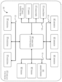
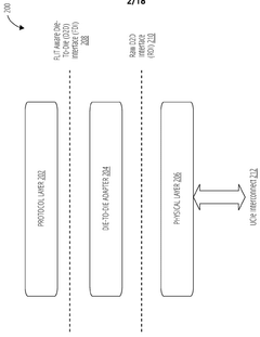
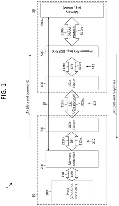
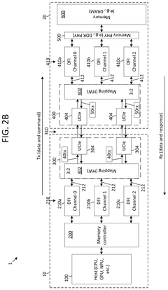
On-package die-to-die (D2D) interconnect for memory using universal chiplet interconnect express (UCIE) phy
PatentWO2024196389A1
Innovation
- The implementation of a Universal Chiplet Interconnect Express (UCIe) PHY for on-package die-to-die interconnects, which enables high-bandwidth, low-latency, and power-efficient connectivity between semiconductor dies, including System-on-a-Chip (SoC) and memory ICs, by mapping standard memory signals to UCIe signals for transport over the UCIe interconnect, thereby scaling memory solutions across various applications from handheld devices to high-performance computing.

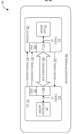
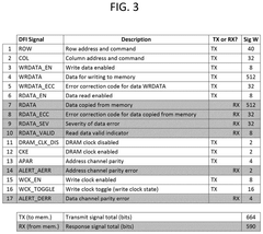
SYSTEMS AND METHODS FOR TRANSMITTING AND RECEIVING DOUBLE DATA RATE (DDR) PHYSICAL (PHY) INTERFACE (DFI) SIGNALS USING UNIVERSAL CHIPLET INTERCONNECT EXPRESS (UCIe)
PatentPendingUS20250258786A1
Innovation
- The use of a universal chiplet interconnect express (UCIe) interface for die-to-die communication, which converts DDR PHY interface signals to UCIe signals based on specific mappings, reducing power consumption and enhancing scalability by integrating fewer UCIe modules compared to traditional DDR PHY methods.

Thermal Management Considerations
Thermal management represents a critical challenge in UCIe Multi-Die Memory systems due to the high-density integration of multiple memory dies. As power density increases with the stacking of memory components, heat dissipation becomes a limiting factor for system performance and reliability. The thermal characteristics of UCIe-based memory architectures differ significantly from traditional single-die configurations, necessitating specialized thermal management strategies.
The primary thermal concerns in UCIe Multi-Die Memory systems stem from the concentrated heat generation in limited physical spaces. With multiple dies operating in close proximity, thermal coupling effects become pronounced, potentially creating hotspots that can degrade performance through thermal throttling mechanisms or even cause permanent damage to sensitive components. Measurements indicate that die-to-die interfaces can experience temperature gradients of 10-15°C under heavy workloads, affecting signal integrity across UCIe links.
Advanced cooling solutions specifically designed for UCIe architectures have emerged as essential components of system design. These include integrated liquid cooling channels between die layers, phase-change materials embedded within the package, and thermally conductive interface materials optimized for multi-die configurations. Recent innovations have demonstrated that targeted cooling solutions can improve thermal performance by up to 30% compared to conventional approaches.
Thermal-aware workload scheduling and power management techniques have also proven effective in mitigating thermal challenges. Dynamic thermal management systems that monitor temperature across multiple dies can redistribute computational and memory access loads to prevent localized overheating. Studies show that intelligent thermal-aware scheduling can reduce peak temperatures by 5-8°C while maintaining comparable bandwidth performance.
The industry has established thermal design power (TDP) guidelines specifically for UCIe Multi-Die Memory implementations, recognizing the unique thermal characteristics of these systems. These guidelines recommend maintaining junction temperatures below 85°C for optimal performance and reliability, with thermal solution designs accounting for worst-case power scenarios across all integrated dies.
Future thermal management approaches for UCIe systems are exploring three-dimensional heat spreading techniques and active cooling solutions integrated directly into the package substrate. These innovations aim to address the increasing thermal challenges as UCIe implementations scale to accommodate higher bandwidth densities and more complex multi-die configurations in next-generation memory systems.
Standardization Efforts and Industry Adoption
The UCIe (Universal Chiplet Interconnect Express) consortium has made significant strides in standardizing multi-die memory interfaces since its formation in 2022. Led by founding members including Intel, AMD, Arm, TSMC, and Samsung, the consortium has established a comprehensive framework for chiplet-to-chiplet communication that addresses bandwidth density, access efficiency, and contention challenges in heterogeneous computing environments.
The initial UCIe 1.0 specification, released in March 2022, focused on establishing the foundational protocols for die-to-die interconnects with particular emphasis on memory access patterns. This specification has since gained widespread adoption across the semiconductor industry, with over 80 member companies now participating in the standardization process.
Industry adoption has accelerated particularly in the high-performance computing and data center segments, where memory bandwidth demands are most acute. Major memory manufacturers including Micron, SK Hynix, and Samsung have announced UCIe-compliant memory solutions, with production timelines extending from 2023 through 2025. These implementations specifically target the bandwidth density and access efficiency requirements outlined in the UCIe standard.
The standardization efforts have evolved to address specific memory contention challenges through the Memory Access Protocol Working Group, established in Q3 2022. This group has developed specifications for quality-of-service mechanisms, memory arbitration, and dynamic bandwidth allocation that are critical for multi-tenant computing environments.
Cloud service providers have emerged as early adopters, with AWS, Google Cloud, and Microsoft Azure all announcing support for UCIe-based memory architectures in their next-generation infrastructure designs. This adoption has been driven by the demonstrable performance improvements in memory-intensive workloads, particularly in AI training and inference applications.
The UCIe Compliance and Interoperability Working Group has established testing methodologies and certification processes to ensure consistent implementation across vendors. The first wave of certified UCIe memory products began appearing in the market in late 2023, with broader availability expected throughout 2024-2025.
Notably, the standardization effort has expanded beyond the initial technical specifications to include power management protocols specifically designed for multi-die memory systems. These protocols enable fine-grained power control across memory dies, addressing one of the key challenges in high-density memory implementations.
The industry adoption roadmap indicates three phases: initial integration in high-end server products (2023-2024), expansion to enterprise computing platforms (2024-2025), and eventual penetration into consumer devices (2025-2026), creating a comprehensive ecosystem for UCIe multi-die memory technologies.
Unlock deeper insights with PatSnap Eureka Quick Research — get a full tech report to explore trends and direct your research. Try now!
Generate Your Research Report Instantly with AI Agent
Supercharge your innovation with PatSnap Eureka AI Agent Platform!