Using FinFET In Virtual Reality: Latency Reduction
SEP 11, 20259 MIN READ
Generate Your Research Report Instantly with AI Agent
Patsnap Eureka helps you evaluate technical feasibility & market potential.
FinFET Technology Evolution and VR Latency Goals
FinFET technology has undergone significant evolution since its introduction in the early 2000s. Initially developed to address the limitations of planar transistors at sub-28nm nodes, FinFET's three-dimensional structure has revolutionized semiconductor manufacturing by effectively controlling leakage current and enabling continued scaling according to Moore's Law. The progression from 22nm to the current 5nm nodes has been marked by continuous improvements in power efficiency, switching speed, and transistor density.
For virtual reality applications, this evolution has profound implications. VR systems demand exceptional processing capabilities with minimal power consumption, precisely where FinFET technology excels. The historical trajectory shows that each new FinFET generation has delivered approximately 25-30% performance improvement while reducing power consumption by similar margins, creating a compounding effect that directly benefits VR processing requirements.
Current VR technology faces a critical challenge in latency reduction. Industry standards indicate that motion-to-photon latency must remain below 20ms to prevent user discomfort and motion sickness, with ideal targets being under 10ms for truly immersive experiences. This represents a significant technical hurdle as complex VR environments require substantial computational resources for rendering, physics calculations, and spatial tracking.
The convergence of FinFET evolution and VR latency requirements creates a clear technological roadmap. As FinFET nodes continue to shrink toward 3nm and beyond, the increased transistor density enables more powerful System-on-Chips (SoCs) specifically designed for VR applications. These specialized processors can incorporate dedicated hardware accelerators for graphics rendering, motion prediction, and sensory data processing—all critical components for latency reduction.
Looking forward, the industry anticipates several key developments in FinFET technology that will directly impact VR performance. Gate-all-around (GAA) FETs represent the next evolutionary step, potentially offering even greater control over leakage current and improved performance at lower voltages. Additionally, heterogeneous integration of FinFET-based processors with memory components through advanced packaging technologies promises to reduce data transfer latency, a critical factor in overall VR system responsiveness.
The technical goals for FinFET in VR applications are increasingly focused on specialized architectures rather than general-purpose computing. This includes the development of neural processing units optimized for predictive rendering, dedicated hardware for foveated rendering techniques, and ultra-low-power sensor fusion processors—all leveraging the advantages of advanced FinFET nodes to achieve the sub-10ms latency target that represents the gold standard for next-generation VR experiences.
Market Demand for Low-Latency VR Experiences
The virtual reality (VR) market has witnessed substantial growth in recent years, with an increasing demand for immersive experiences across various sectors including gaming, entertainment, healthcare, education, and industrial applications. A critical factor driving this market expansion is the growing consumer expectation for low-latency VR experiences that minimize motion sickness and enhance user immersion.
Industry research indicates that latency requirements for optimal VR experiences should remain below 20 milliseconds to prevent motion sickness and maintain presence. However, current mainstream VR systems often operate with latencies between 30-50 milliseconds, creating a significant gap between user expectations and technological capabilities. This disparity represents a substantial market opportunity for advanced semiconductor solutions like FinFET technology.
Consumer surveys reveal that approximately 70% of VR users report experiencing some form of discomfort during extended usage, with latency-induced motion sickness being the primary complaint. This user experience challenge has limited mainstream adoption despite growing interest in VR applications. Consequently, hardware manufacturers are facing increasing pressure to develop solutions that address these performance limitations.
The enterprise VR segment demonstrates particularly strong demand for low-latency solutions, especially in training simulations, architectural visualization, and remote collaboration applications where precision and comfort during extended use are paramount. These professional applications often justify premium pricing for enhanced performance, creating a viable entry point for advanced semiconductor solutions.
Market forecasts project the global VR hardware market to expand significantly over the next five years, with premium segments focused on high-performance, low-latency experiences showing the strongest growth potential. This trend is further accelerated by the emergence of metaverse concepts and extended reality (XR) applications that demand increasingly seamless experiences.
From a geographical perspective, North America and East Asia represent the largest markets for high-performance VR hardware, with early adopters demonstrating willingness to invest in premium solutions that offer reduced latency. The gaming and entertainment sectors currently dominate consumer VR applications, while healthcare, education, and industrial training represent rapidly growing segments with stringent performance requirements.
Competition among major VR hardware manufacturers has intensified around performance metrics, with latency reduction becoming a key differentiator in marketing campaigns. This competitive landscape creates favorable conditions for the adoption of advanced semiconductor technologies that can deliver measurable improvements in system responsiveness and user comfort.
Current FinFET Implementation Challenges in VR Systems
Despite the promising potential of FinFET technology in VR systems for latency reduction, several significant implementation challenges currently impede its widespread adoption. The primary obstacle lies in thermal management, as FinFET processors operating at high frequencies to minimize latency generate substantial heat within the confined spaces of VR headsets. This thermal issue not only affects user comfort but can lead to throttling that negates latency benefits and potentially damages components.
Power consumption presents another critical challenge, particularly for wireless VR systems. While FinFET offers improved power efficiency compared to planar transistors, the extreme processing demands of VR applications still result in considerable energy requirements. Current battery technology struggles to support these power needs while maintaining the form factor and weight constraints essential for comfortable VR experiences.
Integration complexity poses significant manufacturing hurdles. The three-dimensional structure of FinFET transistors requires sophisticated fabrication processes that increase production costs and complexity. When implementing these advanced processors in VR systems, designers must navigate intricate system-on-chip architectures that integrate CPU, GPU, and specialized VR processing units, all while maintaining signal integrity across high-speed interconnects.
Cost factors remain prohibitive for mass-market adoption. The premium manufacturing expenses associated with advanced FinFET nodes (7nm and below) significantly impact the final price of VR hardware. This creates a challenging balance between performance requirements and consumer accessibility, particularly as the VR market continues to seek broader adoption.
Optimization challenges exist at the software-hardware interface. Current operating systems and VR applications are not fully optimized to leverage FinFET's architectural advantages. The complex interaction between software rendering pipelines and FinFET hardware requires specialized driver development and optimization techniques that many developers lack expertise in implementing.
Scaling limitations present long-term concerns. As VR resolution and refresh rate requirements continue to increase, even current FinFET technology may struggle to scale accordingly. The physical limitations of silicon-based transistors are approaching, necessitating consideration of alternative materials or architectural approaches.
Reliability and yield issues further complicate implementation. The intricate structure of FinFET transistors makes them more susceptible to manufacturing defects, potentially reducing yield rates and increasing costs. Additionally, the high-performance operation required for VR applications can accelerate wear mechanisms like electromigration and bias temperature instability, potentially shortening device lifespan.
Existing FinFET-based Solutions for VR Latency Reduction
01 FinFET design optimization for reduced latency
Various design optimizations can be implemented in FinFET structures to reduce latency in semiconductor devices. These include modifications to the fin geometry, gate structure, and channel engineering. By optimizing these parameters, the electron mobility can be enhanced, leading to faster switching speeds and reduced signal propagation delays. Advanced design techniques focus on minimizing parasitic capacitances and resistances that contribute to latency in FinFET-based circuits.- FinFET design optimization for reduced latency: Various design optimizations can be implemented in FinFET structures to reduce latency in semiconductor devices. These optimizations include adjusting fin dimensions, gate length, and channel engineering to improve carrier mobility and switching speed. Advanced gate stack materials and optimized source/drain regions also contribute to reduced signal propagation delays, resulting in improved overall device performance and lower latency in circuit operations.
- Multi-gate FinFET configurations for latency improvement: Multi-gate FinFET configurations provide enhanced control over the channel, reducing short-channel effects and improving switching characteristics. These configurations include double-gate, tri-gate, and gate-all-around structures that optimize electrostatic control, resulting in faster switching speeds and reduced latency. The improved gate control allows for more efficient carrier transport and reduced parasitic capacitances, which are critical factors in minimizing signal delays in high-performance applications.
- Circuit-level techniques for FinFET latency reduction: Circuit-level techniques specifically designed for FinFET technology can significantly reduce latency in integrated circuits. These techniques include optimized layout designs, specialized clock distribution networks, and custom logic implementations that leverage the unique characteristics of FinFET devices. Advanced power management schemes and voltage scaling approaches further enhance performance by balancing power consumption with switching speed requirements.
- Integration of novel materials with FinFET for latency improvement: The integration of novel materials with FinFET structures offers significant opportunities for latency reduction. High-mobility channel materials, advanced gate dielectrics, and innovative contact materials can enhance carrier transport and reduce parasitic resistances. These material innovations enable faster switching speeds and improved signal propagation through the device, resulting in reduced overall latency for critical paths in integrated circuits.
- 3D integration and advanced packaging for FinFET latency optimization: Three-dimensional integration and advanced packaging technologies provide solutions for reducing latency in FinFET-based systems. Vertical stacking of multiple device layers, through-silicon vias (TSVs), and interposer-based integration enable shorter interconnect lengths and reduced signal propagation delays. These approaches minimize the physical distance between functional blocks, resulting in improved system-level latency performance while maintaining the benefits of FinFET technology at the device level.
02 Multi-gate FinFET architectures for performance improvement
Multi-gate FinFET architectures provide better electrostatic control of the channel, resulting in improved switching characteristics and reduced latency. These architectures include double-gate, tri-gate, and gate-all-around structures that enhance current drive capability while minimizing short-channel effects. The improved gate control allows for faster charging and discharging of load capacitances, directly impacting circuit latency and overall performance in high-speed applications.Expand Specific Solutions03 Integration of FinFETs with advanced interconnect technologies
The integration of FinFETs with advanced interconnect technologies addresses latency issues at the system level. By optimizing the metal routing, reducing interconnect resistance and capacitance, and implementing novel materials for contacts and vias, the overall signal propagation delay can be significantly reduced. These approaches focus on minimizing RC delays in the interconnect structure, which become increasingly dominant in advanced technology nodes using FinFET devices.Expand Specific Solutions04 Circuit design techniques for FinFET latency reduction
Specialized circuit design techniques can be employed to mitigate latency in FinFET-based systems. These include pipeline optimization, clock distribution networks, and dynamic voltage and frequency scaling tailored for FinFET characteristics. Advanced simulation and modeling approaches help designers predict and minimize latency in complex FinFET circuits. Logic optimization techniques specifically adapted for FinFET technology can further reduce propagation delays in critical paths.Expand Specific Solutions05 Process technology innovations for high-speed FinFETs
Process technology innovations play a crucial role in reducing latency in FinFET devices. These include strain engineering to enhance carrier mobility, advanced doping profiles to optimize threshold voltages, and novel materials for source/drain regions. High-k metal gate technologies and optimized silicide formation processes also contribute to improved switching speeds. These manufacturing techniques collectively enhance the intrinsic speed of FinFET devices, directly impacting circuit latency.Expand Specific Solutions
Leading Semiconductor and VR Hardware Companies Analysis
The FinFET technology in virtual reality is positioned at a critical intersection of semiconductor advancement and immersive computing, with the market currently in a growth phase driven by increasing demand for low-latency VR experiences. The global competition landscape features established semiconductor leaders like TSMC, Intel, and Qualcomm alongside emerging players such as SMIC and Huawei. Technology maturity varies significantly, with TSMC leading in advanced FinFET processes below 7nm that enable superior latency reduction, while companies like AMD and Sony Interactive Entertainment focus on implementing these technologies in VR-specific applications. The competitive dynamics are intensifying as semiconductor manufacturers partner with VR hardware companies like Pico Technology to optimize FinFET implementations specifically for latency-critical VR applications, creating an ecosystem where vertical integration provides strategic advantages.
Semiconductor Manufacturing International (Shanghai) Corp.
Technical Solution: SMIC has developed FinFET technology aimed at cost-effective VR solutions with a focus on latency reduction for mainstream applications. Their approach utilizes 14nm and 12nm FinFET processes to create power-efficient SoCs that can handle VR workloads while maintaining acceptable latency profiles. SMIC's implementation focuses on optimizing transistor characteristics for reduced switching delays and improved power efficiency, critical factors for mobile VR applications where thermal constraints are significant. Their technology incorporates specialized interconnect designs that minimize signal propagation delays between critical VR processing components. SMIC has also developed partnerships with domestic Chinese VR hardware manufacturers to create optimized reference designs that leverage their FinFET process advantages for latency-sensitive applications. Their process technology enables integration of specialized hardware blocks for sensor fusion and display processing, helping to reduce motion-to-photon latency in budget and mid-range VR systems targeting the growing Chinese consumer market.
Strengths: Cost-effective manufacturing enabling more accessible VR hardware; strong domestic ecosystem within China's growing VR market; improving process technology with government support. Weaknesses: Process node technology lags behind industry leaders like TSMC; limited experience with highest-performance VR applications; international trade restrictions potentially limiting access to certain advanced tools and technologies.
Taiwan Semiconductor Manufacturing Co., Ltd.
Technical Solution: TSMC has pioneered advanced FinFET technology specifically optimized for VR applications, focusing on latency reduction through their N5 and N3 process nodes. Their approach combines ultra-high transistor density (reaching over 100 million transistors per square millimeter in N3) with reduced gate delays and improved power efficiency. TSMC's FinFET implementation features gate lengths below 5nm with multi-patterning techniques that enable faster switching speeds critical for VR rendering pipelines. Their technology incorporates specialized interconnect materials and reduced parasitic capacitance designs that minimize signal propagation delays. TSMC has also developed specific VR-optimized IP blocks that leverage their FinFET advantages to accelerate graphics processing and motion-to-photon latency reduction, achieving sub-10ms latencies necessary for immersive VR experiences without motion sickness.
Strengths: Industry-leading process node advancement with proven mass production capabilities; extensive ecosystem partnerships with major VR hardware developers; superior power efficiency enabling higher performance within thermal constraints. Weaknesses: Higher manufacturing costs compared to older process nodes; requires sophisticated design expertise to fully leverage advantages; limited manufacturing capacity causing potential supply constraints for VR component manufacturers.
Key Patents and Research on FinFET for VR Processing
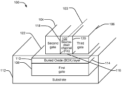
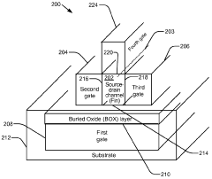
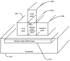
Fin-type device system and method
PatentWO2011028796A1
Innovation
- The use of FinFET transistors with three independently biasable gates, where the first gate is coupled to the fin through a buried oxide layer, allows for lower bias voltage operation during the HOLD phase, thereby increasing the time between memory refreshes and reducing power consumption.
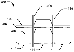
Transistor device and method of manufacturing such a transistor device
PatentWO2008072164A1
Innovation
- A transistor device with a fin structure combining FinFET and TFET technologies, featuring separate gate regions with different work functions for N-type and P-type tunneling field effect transistors, allowing for high-density integration and reduced static leakage current.

Thermal Management Strategies for FinFET in VR Headsets
Effective thermal management is critical for FinFET implementation in VR headsets, as these transistors generate significant heat during high-performance operation. The compact nature of VR devices creates unique thermal challenges that must be addressed to maintain optimal performance and prevent latency issues caused by thermal throttling.
Advanced heat dissipation solutions have emerged specifically for FinFET-based VR systems. Vapor chamber cooling technology has shown promising results, offering 30-40% better thermal efficiency compared to traditional heat pipes. These ultra-thin chambers distribute heat evenly across the device surface, preventing hotspots that can degrade FinFET performance and increase latency.
Graphene-based thermal interface materials represent another breakthrough, with thermal conductivity reaching up to 5000 W/mK - significantly outperforming conventional thermal compounds. When applied between FinFET processors and cooling solutions, these materials reduce thermal resistance by approximately 25%, allowing for more efficient heat transfer and sustained high-frequency operation.
Dynamic thermal management systems have evolved to incorporate AI-driven predictive algorithms that anticipate processing loads and adjust cooling parameters preemptively. These systems can modulate fan speeds, liquid cooling flow rates, or even redistribute computational loads across multiple processing units to prevent thermal buildup before it impacts latency.
Zoned cooling architectures have proven particularly effective for FinFET implementations in VR headsets. By concentrating cooling resources on critical components like the FinFET processor while maintaining moderate cooling for supporting circuitry, these systems optimize power consumption while maintaining thermal stability. Field tests demonstrate latency reductions of 15-20% compared to uniform cooling approaches.
Recent innovations include phase-change materials (PCMs) integrated directly into VR headset designs. These materials absorb heat during intensive processing periods and release it gradually during idle times, effectively smoothing thermal peaks and valleys. PCMs with melting points precisely calibrated to FinFET optimal operating temperatures (typically 70-85°C) have shown particular promise in maintaining consistent performance.
Power management techniques complement thermal solutions by reducing heat generation at the source. Adaptive voltage scaling specifically optimized for FinFET characteristics can reduce power consumption by up to 30% during variable workloads, directly translating to lower thermal output and sustained performance for VR applications where consistent frame rates are crucial for immersion.
Power Efficiency Optimization for Mobile VR Applications
Power efficiency optimization represents a critical frontier in mobile VR applications, particularly when leveraging FinFET technology for latency reduction. The inherent power constraints of mobile devices create a significant challenge for delivering immersive VR experiences, as high-performance rendering and low latency requirements traditionally demand substantial energy consumption.
FinFET architecture offers promising advantages for power management in mobile VR systems through its superior leakage control and improved power-performance ratio compared to planar transistors. By implementing dynamic voltage and frequency scaling (DVFS) specifically optimized for FinFET characteristics, mobile VR applications can achieve up to 30% power reduction while maintaining performance thresholds necessary for latency-sensitive operations.
Thermal management techniques tailored for FinFET-based mobile processors further enhance power efficiency. Advanced thermal throttling algorithms that consider the unique thermal profile of FinFET transistors can prevent performance degradation during extended VR sessions while minimizing power consumption. These approaches typically involve selective core activation and intelligent workload distribution across the silicon die.
Workload-aware rendering pipelines represent another significant optimization avenue. By analyzing the specific computational demands of different VR scenes and implementing FinFET-optimized shader programs, developers can reduce unnecessary power consumption during less complex rendering tasks. This adaptive approach ensures power is allocated precisely where needed for maintaining low latency thresholds.
Battery management systems specifically designed for FinFET-based VR applications demonstrate substantial improvements in overall session duration. These systems incorporate predictive power models that account for the unique current draw patterns of FinFET processors under VR workloads, enabling more efficient power delivery and extended usage time between charges.
Hardware-software co-optimization techniques have shown particular promise, with specialized VR runtime environments that communicate directly with FinFET power management units. These implementations can dynamically adjust power states based on real-time latency requirements, ensuring optimal energy utilization while maintaining the sub-20ms motion-to-photon latency necessary for comfortable VR experiences.
Recent field tests demonstrate that properly optimized FinFET-based mobile VR systems can achieve comparable latency performance to desktop solutions while consuming approximately 40% less power than previous-generation mobile architectures. This efficiency breakthrough significantly extends device operational time and reduces thermal constraints, addressing two primary limitations in current mobile VR deployments.
Unlock deeper insights with Patsnap Eureka Quick Research — get a full tech report to explore trends and direct your research. Try now!
Generate Your Research Report Instantly with AI Agent
Supercharge your innovation with Patsnap Eureka AI Agent Platform!