

MEMS technology preparation method of piezoelectret matrix
A piezoelectric electret and matrix technology, which is applied in the process of producing decorative surface effects, metal material coating process, decorative art, etc., can solve the problem of low preparation efficiency and achieve the effect of free and flexible regulation
Patent Information
- Authority / Receiving Office
- CN · China
- Current Assignee / Owner
- Publication Date
- 2015-11-11
Smart Images
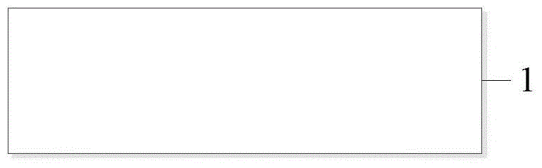
Figure 1 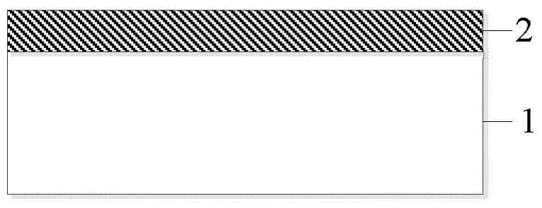
Figure 2 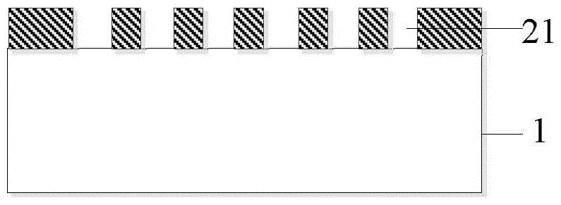
Figure 3
Abstract
Description
technical field
[0001] The invention relates to micromachining preparation technology, in particular to a method for preparing a piezoelectric electret matrix with MEMS technology. Background technique
[0002] Piezoelectric electret is a new type of flexible porous electret with strong piezoelectric effect. Its piezoelectric constant d 33 It can reach hundreds of pC / N, and its piezoelectric performance is comparable to that of traditional piezoelectric ceramic materials. It is widely used in the field of micro-electromechanical systems, especially in acoustic / vibration / pressure sensors. The piezoelectric electret includes the piezoelectric electret matrix and the polarized charges on its surface. The piezoelectric electret matrix is a porous structure, and there are polarized charges attached near the holes of the piezoelectric electret matrix; under the action of external force , the shape of the piezoelectric electret changes, resulting in a piezoelectric effect. The...
Examples
Embodiment Construction
[0028] The present invention will be further described through the embodiments below in conjunction with the accompanying drawings.
[0029] The preparation method of the MEMS process of the piezoelectric electret substrate of the present embodiment, comprises the following steps:
[0030] 1) Provide the substrate 1, the material is Si, and the thickness is 400 μm, such as figure 1 shown;
[0031] 2) Spin-coat photoresist 2 on the substrate. The photoresist is AZP4620 with a thickness of 7 μm. Use a hot oven to soft-bake the photoresist at a temperature of 150 ° C for 25 minutes. figure 2 shown;
[0032] 3) According to the pattern of the holes of the required piezoelectric electret substrate designed on the first photoresist plate, the pattern of the first photoresist plate is transferred to the photoresist by ultraviolet exposure, the exposure time is 9 seconds, and the development time is 1.5 seconds. Minutes, just can form the figure 21 of required hole on photoresist...