
Display device, array substrate and manufacturing method thereof
A technology for array substrates and connection layers, which is applied in semiconductor/solid-state device manufacturing, semiconductor devices, electrical components, etc., and can solve problems such as poor display
Patent Information
- Authority / Receiving Office
- CN · China
- Patent Type
- Patents(China)
- Current Assignee / Owner
- Publication Date
- 2020-02-21
Smart Images
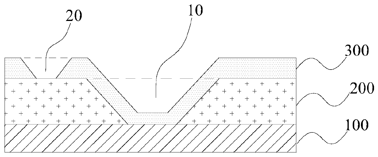
Figure 1 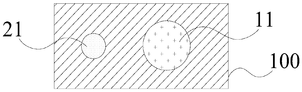
Figure 2 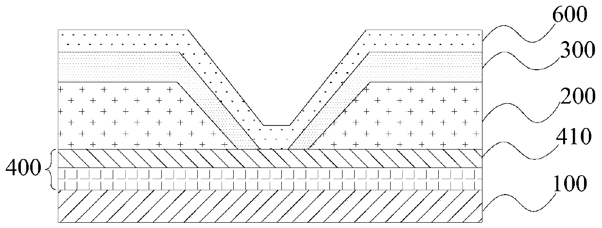
Figure 3
Abstract
Description
technical field
[0001] The present invention relates to the field of display technology, in particular, to a display device, an array substrate and a preparation method thereof. Background technique
[0002] Thin Film Transistor Liquid Crystal Display (TFT-LCD) is a type of liquid crystal display that uses thin film transistor technology to improve image quality, display quality and overall performance. TFT-LCD is favored by people for its large capacity, high definition and high-quality true color, and is widely used in TVs, flat-panel displays, projectors and electronic equipment. TFT-LCD uses an array substrate and a color film substrate to form a liquid crystal cell, and then undergoes subsequent processes such as polarizer coating, and finally forms a liquid crystal display device. Among them, the array substrate is one of the important components of the TFT-LCD.
[0003] However, the current display devices, array substrates and manufacturing methods thereof still ne...
Examples
Embodiment Construction
[0030] Embodiments of the present invention are described in detail below, examples of which are shown in the drawings, wherein the same or similar reference numerals designate the same or similar elements or elements having the same or similar functions throughout. The embodiments described below by referring to the figures are exemplary only for explaining the present invention and should not be construed as limiting the present invention.
[0031] In one aspect of the present invention, the present invention provides an array substrate. According to an embodiment of the present invention, refer to figure 1 , the array substrate includes: a substrate 100 , a planarization layer 200 and a passivation layer 300 . According to an embodiment of the present invention, a planarization layer 200 is disposed on the substrate 100 . According to an embodiment of the present invention, the planarization layer 200 has a first via hole 10 . According to an embodiment of the present in...