

Pixel driving circuit and method, and display device
A pixel driving circuit and pixel technology, applied in static indicators, instruments, etc., can solve the problems of low light transmittance, white screen, white display screen, etc., to improve scanning speed, avoid display screen white, Solve the effect of whitening the display screen
Patent Information
- Authority / Receiving Office
- CN · China
- Patent Type
- Applications(China)
- Current Assignee / Owner
- Publication Date
- 2018-11-02
Smart Images
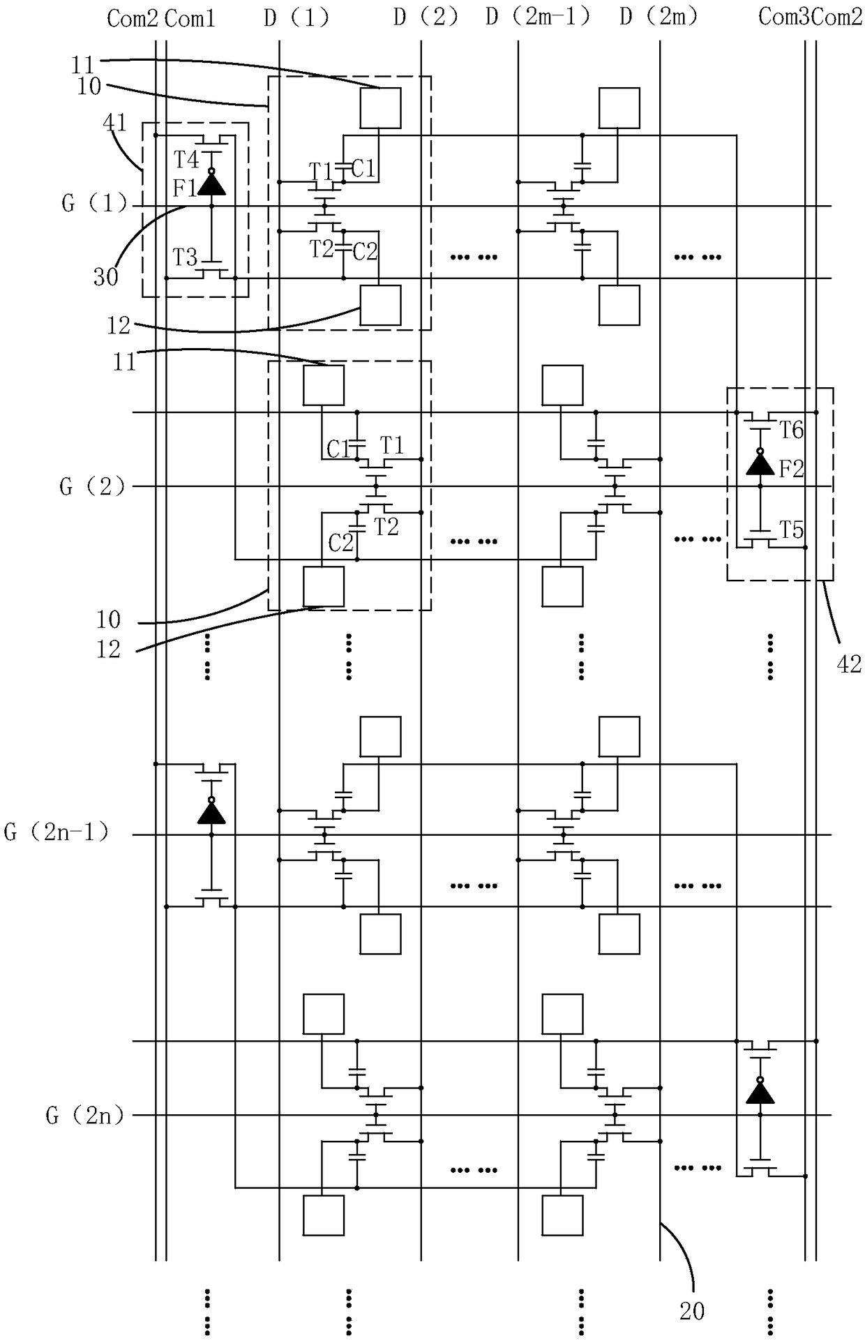
Figure 1 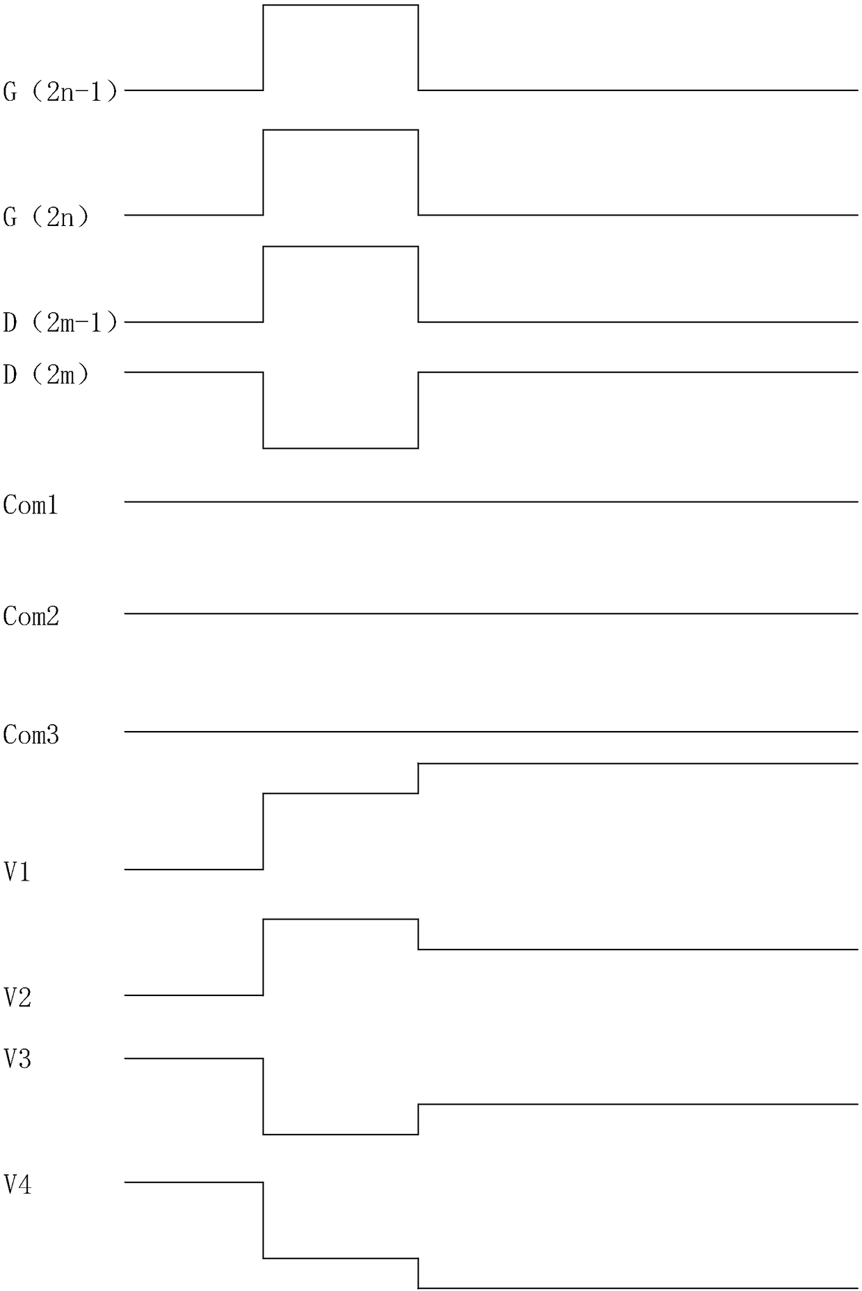
Figure 2 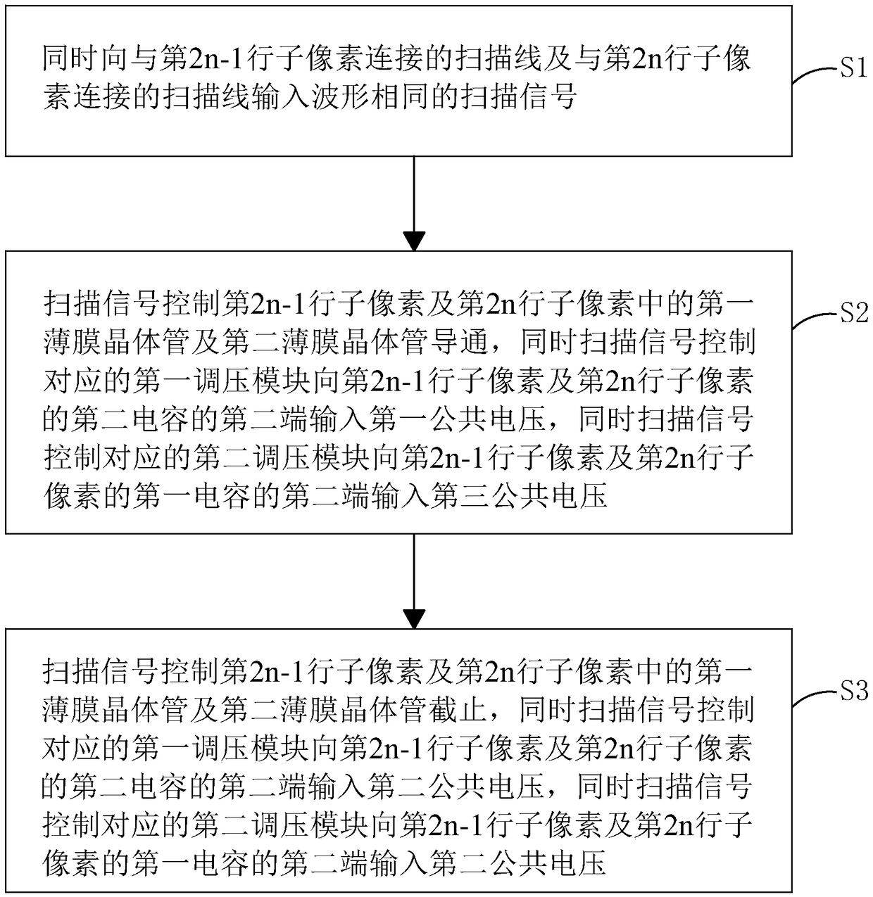
Figure 3
Abstract
Description
technical field
[0001] The invention relates to the technical field of liquid crystal display, in particular to a pixel driving circuit, a pixel driving method and a display device. Background technique
[0002] A liquid crystal display device (Liquid Crystal Display, LCD) is one of the most widely used flat panel displays at present, and a liquid crystal panel is a core component of the liquid crystal display device. A liquid crystal panel usually consists of a color filter substrate (Color Filter Substrate, CF Substrate), a thin film transistor array substrate (Thin FilmTransistor Array Substrate, TFT Array Substrate), and a liquid crystal layer (Liquid Crystal Layer) arranged between the two substrates. constituted. Generally, pixel electrodes and common electrodes are respectively arranged on the array substrate and the color filter substrate. When a voltage is applied to the pixel electrode and the common electrode, an electric field will be generated in the liquid cr...
Examples
Embodiment Construction
[0031] In order to further illustrate the technical means adopted by the present invention and its effects, the following describes in detail in conjunction with preferred embodiments of the present invention and accompanying drawings.
[0032] see figure 1 and figure 2 , the present invention provides a pixel driving circuit, including a plurality of sub-pixels 10 arranged in an array, a plurality of data lines 20 (D(1), D(2)...D(2m-1), D(2m)... ) and scanning lines 30 (G(1), G(2)...G(2n-1), G(2n)...), a plurality of first voltage regulation modules 41 and a plurality of second voltage regulation modules 42.
[0033] Each scanning line 30 is correspondingly connected to a row of sub-pixels 10; a column of sub-pixels 10 is correspondingly connected to two data lines 20, and the odd-numbered row of sub-pixels 10 in the column of sub-pixels 10 is connected to one of the corresponding two data lines 20. The sub-pixels 10 in even rows in 10 are connected to the other one of the c...