
Organic light-emitting device and method of manufacturing organic light-emitting device
A technology of organic light-emitting devices and organic layers, which is applied in the direction of organic semiconductor devices, semiconductor/solid-state device manufacturing, and electric solid-state devices. It can solve problems such as poor electrical conductivity, improve external quantum efficiency, and achieve normal luminous effects.
Patent Information
- Authority / Receiving Office
- CN · China
- Current Assignee / Owner
- Publication Date
- 2021-04-02
Smart Images
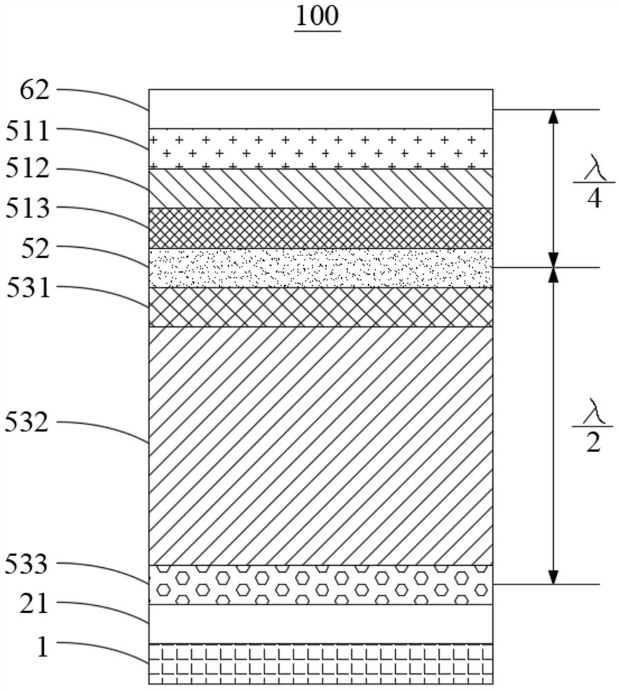
Figure 1 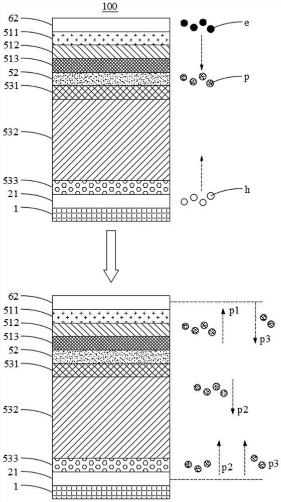
Figure 2 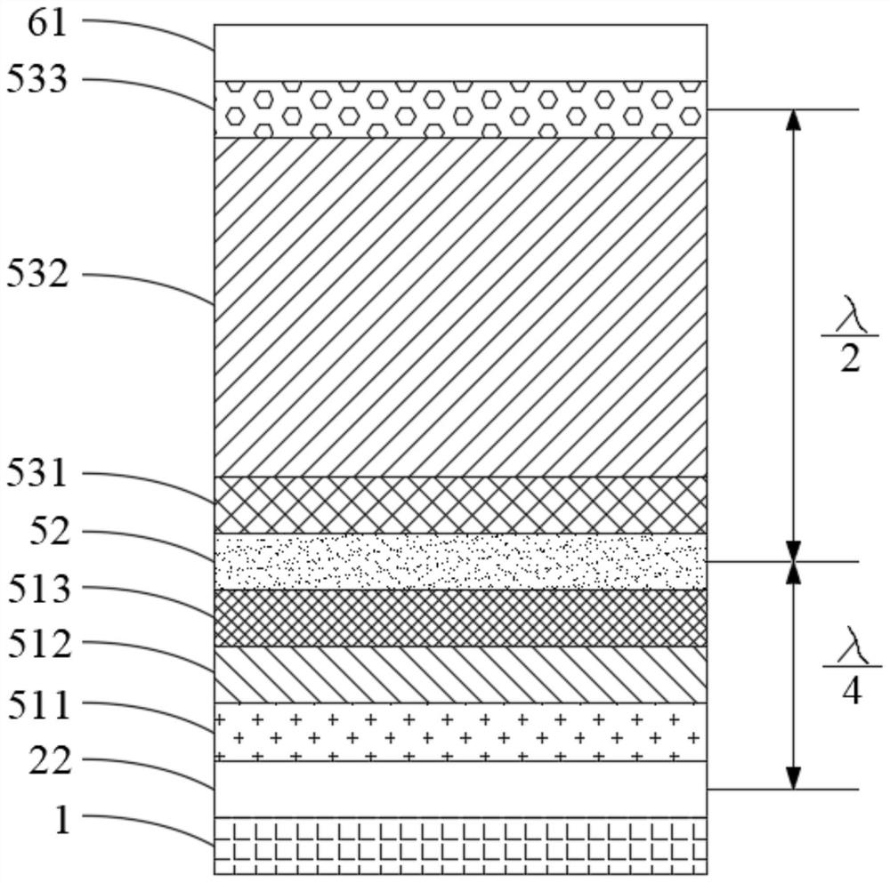
Figure 3
Abstract
Description
technical field
[0001] The invention belongs to the field of display technology, and in particular relates to an organic light-emitting device and a method for manufacturing the organic light-emitting device. Background technique
[0002] In a manufacturing process of an OLED (Organic Light-Emitting Diode, organic light-emitting device) display panel, in order to match a thin film transistor (Thin Film Transistor, TFT) with higher mobility, it is necessary to perform an inverted design on the OLED device to form an inverted OLED device. However, when using an inverted OLED device, generally a higher voltage needs to be applied to ensure that the inverted OLED device can emit light normally. Contents of the invention
[0003] In view of this, the present invention provides an organic light-emitting device and a method for manufacturing the organic light-emitting device. On the basis of adding a transparent organic layer to the organic light-emitting device, a conductive lay...
Examples
Embodiment Construction
[0033] In order to make the object, technical solution and advantages of the present invention clearer, the present invention will be further described in detail below in conjunction with the accompanying drawings and embodiments. It should be understood that the specific embodiments described here are only used to explain the present invention, not to limit the present invention.
[0034] In describing the present invention, it is to be understood that the terms "central", "lateral", "upper", "lower", "left", "right", "vertical", "horizontal", "top", The orientation or positional relationship indicated by "bottom", "inner" and "outer" is based on the orientation or positional relationship shown in the drawings, and is only for the convenience of describing the present invention and simplifying the description, rather than indicating or implying the referred device Or elements must have a certain orientation, be constructed and operate in a certain orientation, and thus should...