
Flat panel detector pixel structure and manufacturing method thereof
A flat-panel detector and pixel structure technology, which is applied in the direction of electric solid-state devices, semiconductor devices, radiation control devices, etc., can solve the problems of difficult operation of pixels, sharp increase of leakage current of flat-panel detector pixels, and unstable working performance, so as to avoid edge Discharge, reduce surface leakage, eliminate the effect of discharge
Patent Information
- Authority / Receiving Office
- CN · China
- Patent Type
- Applications(China)
- Current Assignee / Owner
- Publication Date
- 2021-10-22
Smart Images
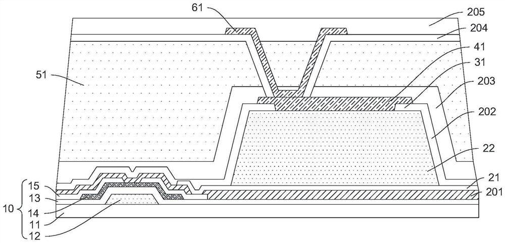
Figure 1 
Figure 2 
Figure 3
Abstract
Description
technical field
[0001] The invention relates to the technical field of semiconductor devices, in particular to a flat panel detector pixel structure and a manufacturing method thereof. Background technique
[0002] At present, flat-panel detectors are widely used in medical imaging, industrial non-destructive testing, security inspection and other fields. The size can reach tens of centimeters, and the pixel substrate can be composed of millions or even tens of millions of pixel unit circuits. In different application fields, different requirements are often put forward for the performance of flat panel detectors. For example, in some application scenarios, flat panel detectors are required to work under a relatively high negative bias voltage. Although there are currently some products that can work under negative bias voltage, the working performance is not stable enough; as the negative bias voltage increases, the leakage current of the flat panel detector pixel will inc...
Examples
Embodiment Construction
[0045] Hereinafter, embodiments of the present disclosure will be described with reference to the drawings. It should be understood, however, that these descriptions are exemplary only, and are not intended to limit the scope of the present disclosure. Also, in the following description, descriptions of well-known structures and techniques are omitted to avoid unnecessarily obscuring the concept of the present disclosure.
[0046] Various structural schematic diagrams according to embodiments of the present disclosure are shown in the accompanying drawings. The figures are not drawn to scale, with certain details exaggerated and possibly omitted for clarity of presentation. The shapes of the various regions and layers shown in the figure, as well as their relative sizes and positional relationships are only exemplary, and may deviate due to manufacturing tolerances or technical limitations in practice, and those skilled in the art will Regions / layers with different shapes, s...