
System and method of silicon switched power delivery using a package
a technology of switching power and package, applied in the direction of logic circuit, semiconductor/solid-state device details, pulse technique, etc., can solve the problems of increasing routing complexity, increasing power consumption of circuitry, and small circuitry, so as to reduce current leakage, simplify the placement of components on the substrate, and improve the effect of voltage level
Patent Information
- Authority / Receiving Office
- US · United States
- Patent Type
- Applications(United States)
- Current Assignee / Owner
- Publication Date
- 2007-11-15
Smart Images
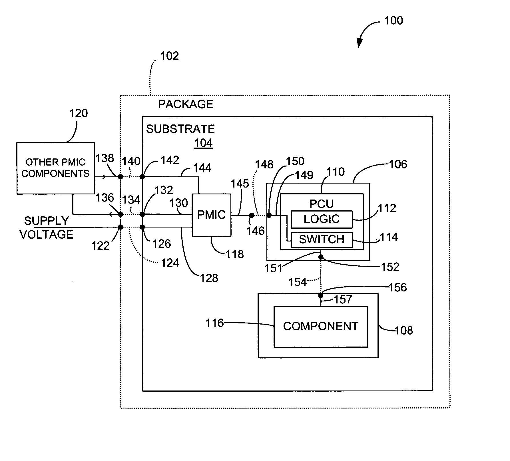
Figure 1 
Figure 2 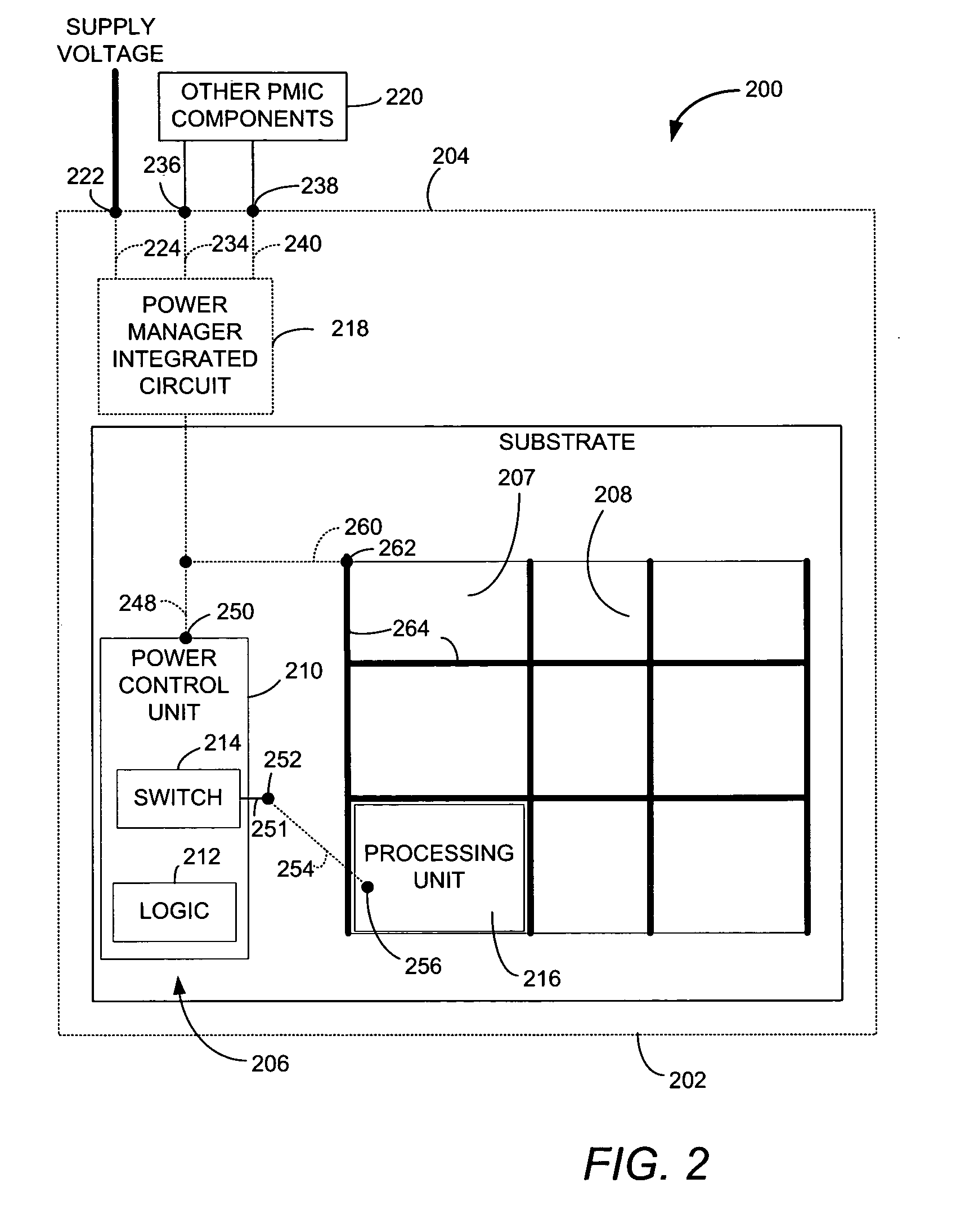
Figure 3
Abstract
Description
BACKGROUND
[0001] I. Field
[0002] The present disclosure generally relates to systems and methods of power distribution in a circuit, and more particularly to systems and methods using low-resistance package metals to distribute switched power or signals to designated areas of a silicon substrate.
[0003] II. Description of Related Art
[0004] Advances in technology have resulted in smaller and more powerful personal computing devices. For example, a variety of portable personal computing devices, including wireless computing devices, such as portable wireless telephones, personal digital assistants (PDAs), and paging devices are small, lightweight, and easily carried by users. More specifically, portable wireless telephones, such as cellular (analog and digital) telephones and IP telephones, can communicate voice and data packets over wireless networks. Further, many such wireless telephones include other types of devices that are incorporated therein. For example, a wireless telepho...
Examples
Embodiment Construction
[0040] In a particular embodiment, a control unit within first domain of a substrate may utilize a metallization portion of an off-substrate package to selectively route power, signals, or a combination thereof to a second domain of the substrate that is electrically isolated from the first domain. The second domain may include, for example, an electrical component such as a processor, a memory, other integrated circuit resources, and the like. In integrated circuitry, the voltage efficiencies often have a significant impact overall performance. By routing power and signals through the off-substrate package, the control unit may reduce voltage loss by taking advantage of the metallization of the package, which typically has a lower electrical resistance than metal traces within the substrate. The control unit may route power or shut off power to selected components to activate or deactivate components of the substrate. In some instances, the activation and deactivation of components...