
Impedance mating interface for electrical connectors
a technology of impedance mating and electrical connectors, which is applied in the direction of coupling device connection, connection contact member material, coupling protective earth/shielding arrangement, etc., can solve the problems of increasing impedance, and achieve the effect of improving performance, maximizing capacitance, and minimizing impedan
Patent Information
- Authority / Receiving Office
- US · United States
- Patent Type
- Applications(United States)
- Current Assignee / Owner
- Publication Date
- 2009-07-30
Smart Images
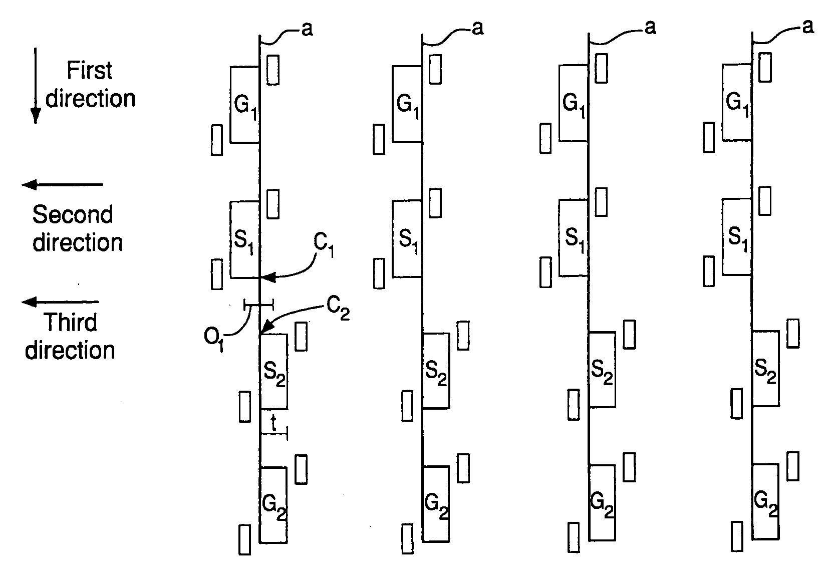
Figure 1 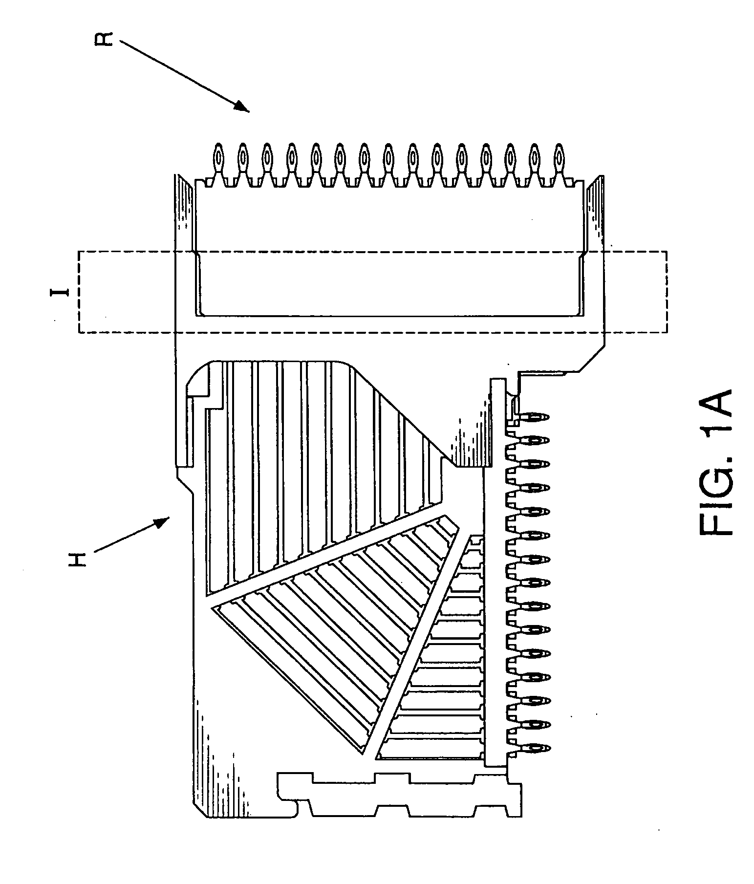
Figure 2 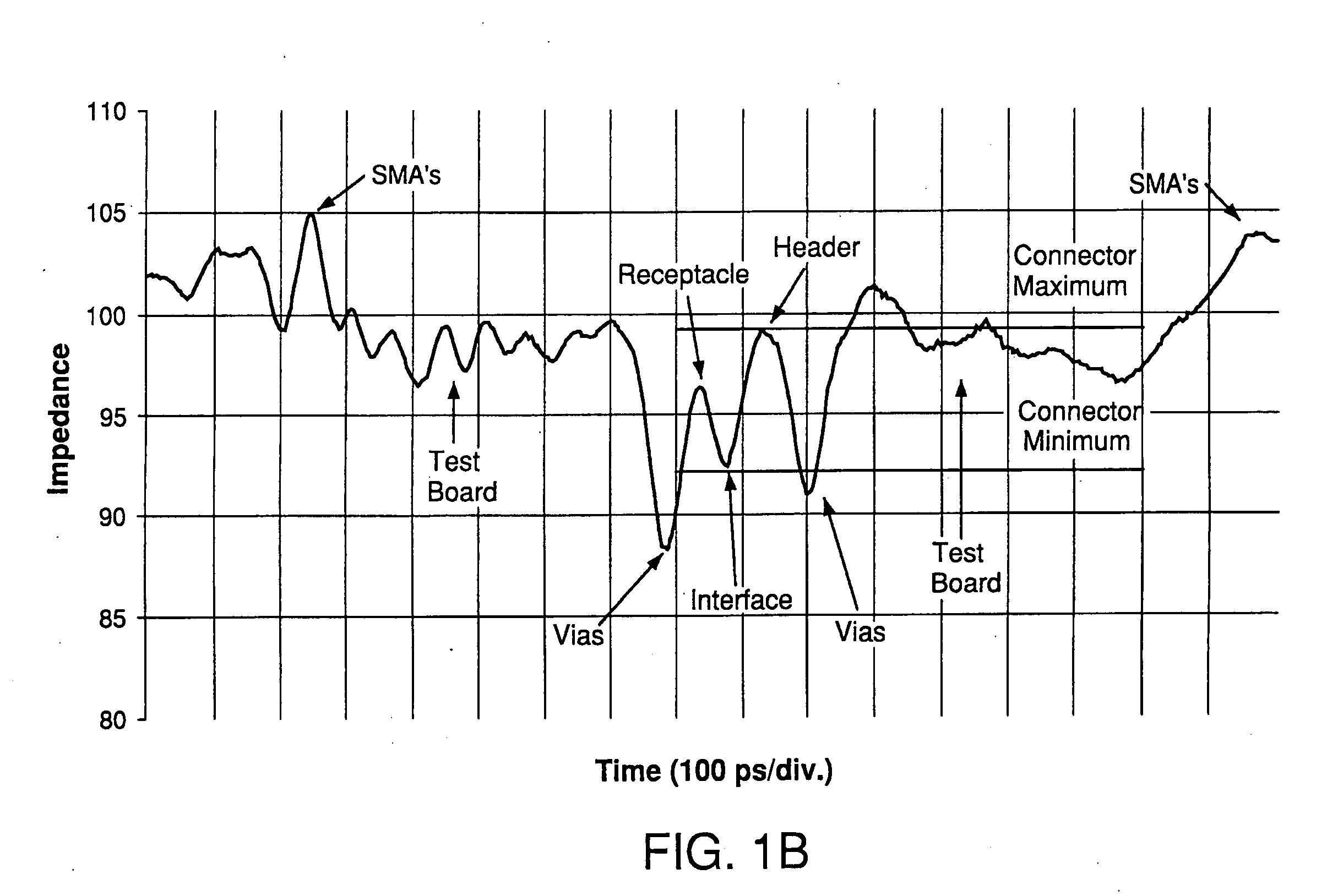
Figure 3
Abstract
Description
CROSS-REFERENCE TO RELATED APPLICATIONS
[0001] This is a divisional patent application of U.S. patent application Ser. No. 11 / 229,778 filed on Sep. 19, 2005, which is a continuation-in-part of U.S. patent application Ser. No. 10 / 946,874 filed on Sep. 22, 2004, which in-turn claims the benefit under 35 U.S.C. § 119(e) of provisional U.S. patent application No. 60 / 506,427, filed Sep. 26, 2003.
[0002] The subject matter disclosed herein is related to the subject matter disclosed and claimed in U.S. patent application Ser. No. 10 / 634,547, filed Aug. 5, 2003, entitled “Electrical connectors having contacts that may be selectively designated as either signal or ground contacts,” and in U.S. patent application Ser. No. 10 / 294,966, filed Nov. 14, 2002, which is a continuation-in-part of U.S. patent applications No. 09 / 990,794, filed Nov. 14, 2001, now U.S. Pat. No. 6,692,272, and Ser. No. 10 / 155,786, filed May 24, 2002, now U.S. Pat. No. 6,652,318.
[0003] The disclosure of each of the above-refer...
Examples
Embodiment Construction
[0019]FIGS. 2A and 2B depict example embodiments of a header connector. As shown, the header connector 200 may include a plurality of insert molded lead frame assemblies (IMLAs) 202. FIGS. 3A and 3B are side views of example embodiments of an IMLA 202 according to the invention. An IMLA 202 includes a contact set 206 of electrically conductive contacts 204, and an IMLA frame 208 through which the contacts 204 at least partially extend. An IMLA 202 may be used, without modification, for single-ended signaling, differential signaling, or a combination of single-ended signaling and differential signaling. Each contact 204 may be selectively designated as a ground contact, a single-ended signal conductor, or one of a differential signal pair of signal conductors. The contacts designated G may be ground contacts, the terminal ends of which may be extended beyond the terminal ends of the other contacts. Thus, the ground contacts G may mate with complementary receptacle contacts before any...