
Liquid crystal display device and method for manufacturing the same
a liquid crystal display and liquid crystal technology, applied in non-linear optics, instruments, optics, etc., can solve the problems of uneven display defective operation, easy cracking of element formation layers including semiconductor elements, etc., to reduce the damage of liquid crystal display devices by local charging, reduce image quality, and reduce the effect of stress due to bending
Patent Information
- Authority / Receiving Office
- US · United States
- Patent Type
- Applications(United States)
- Current Assignee / Owner
- Publication Date
- 2010-01-14
- Estimated Expiration
- Not applicable · inactive patent
Smart Images
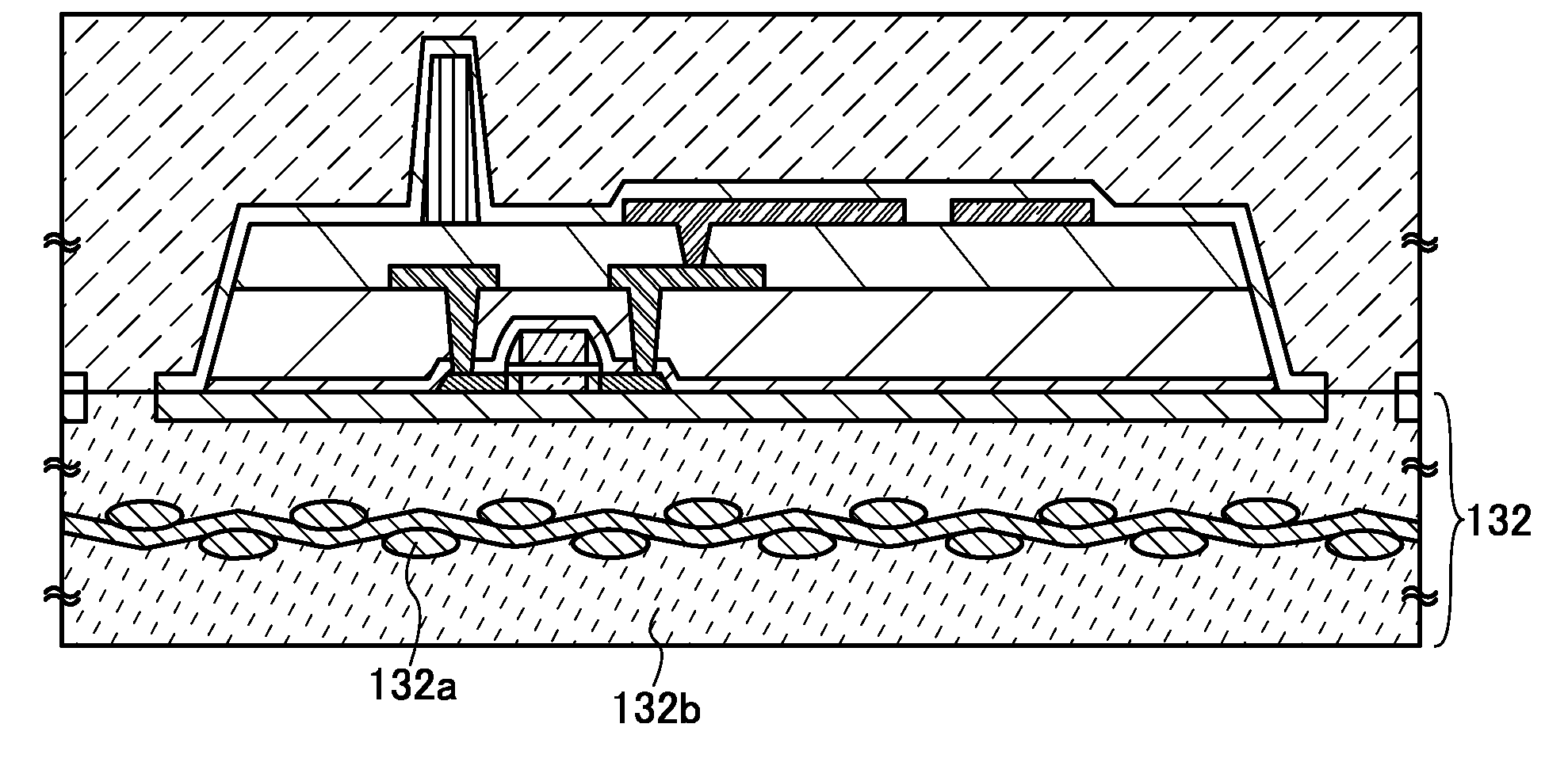
Figure 1 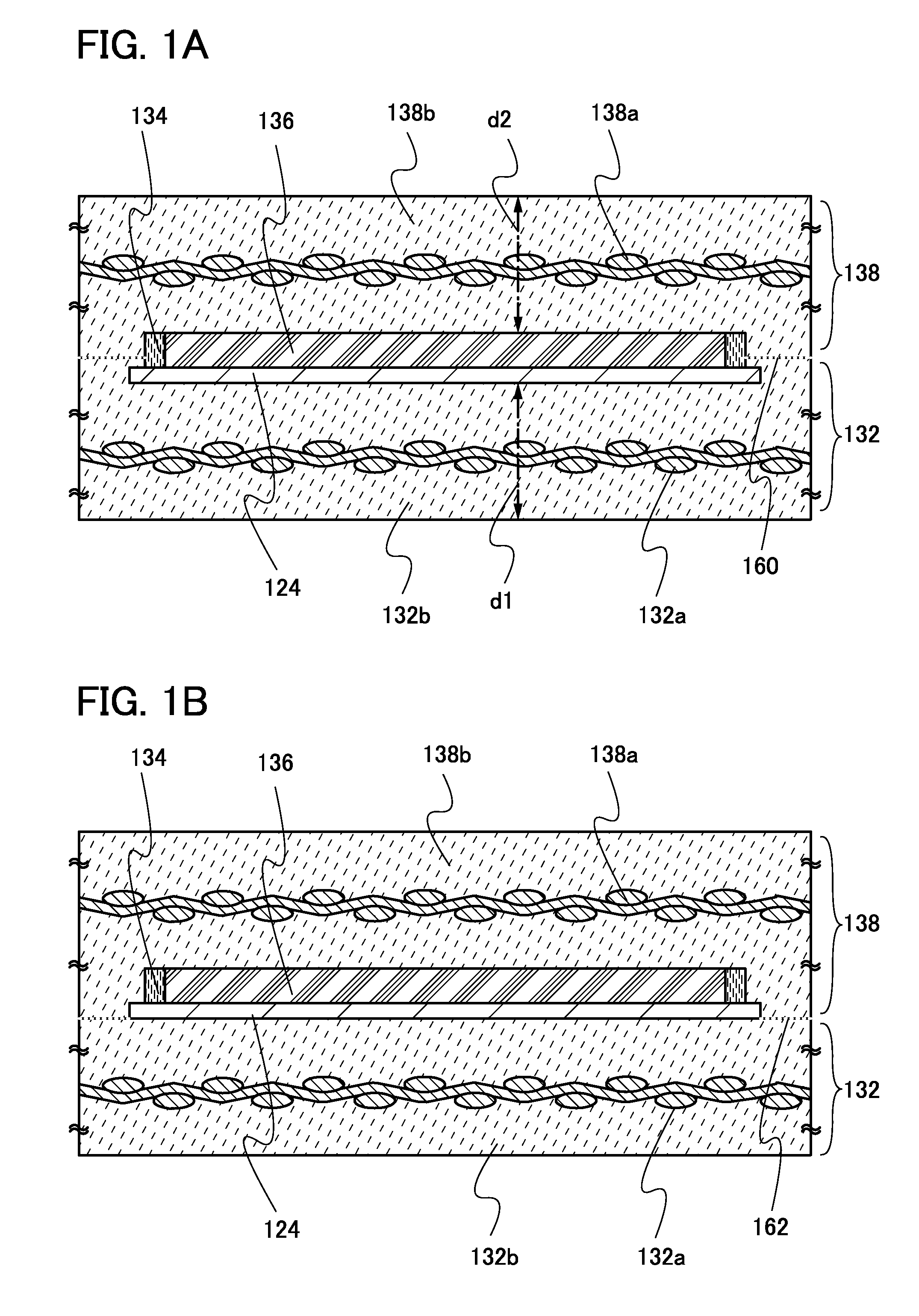
Figure 2 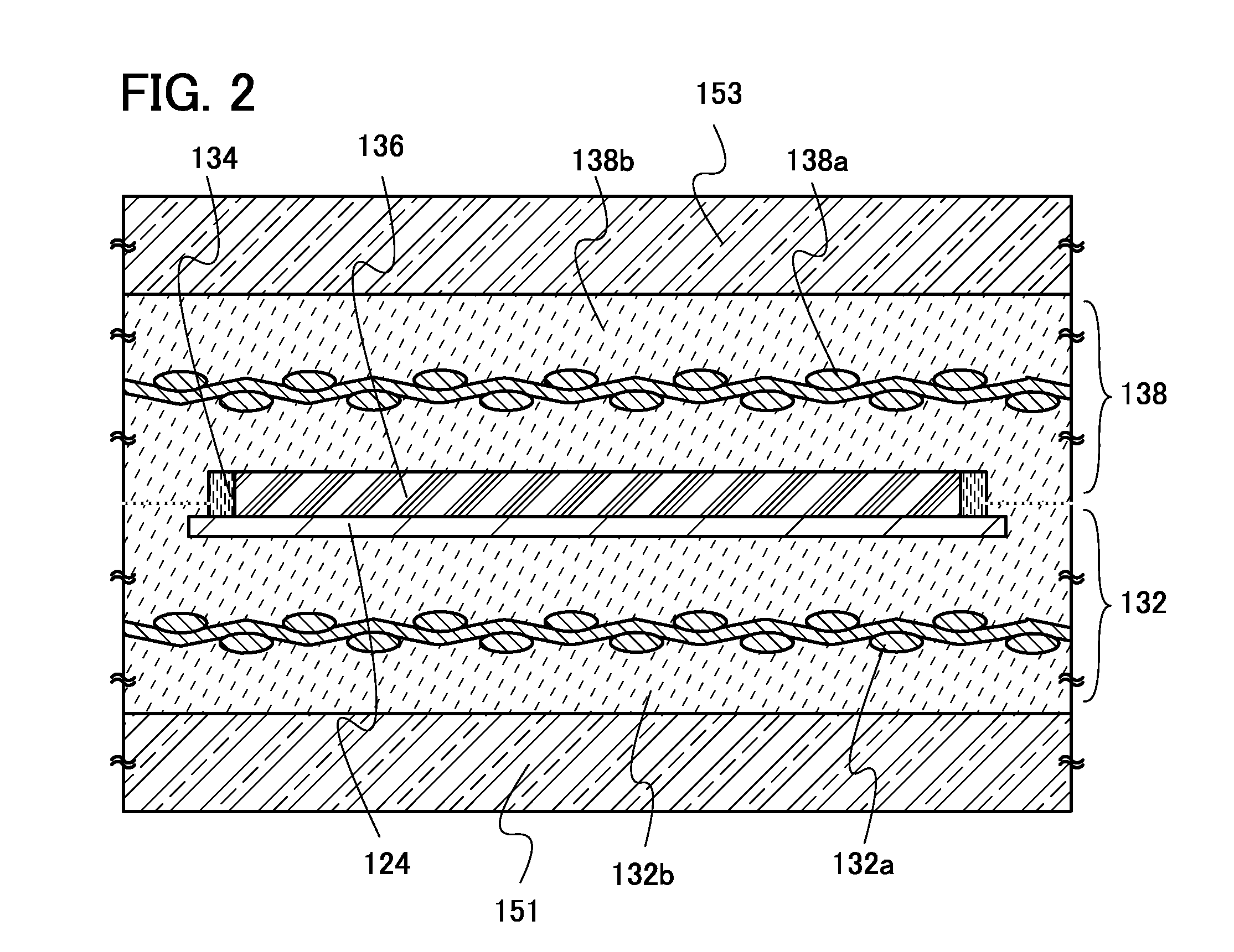
Figure 3
Abstract
Description
BACKGROUND OF THE INVENTION
[0001] 1. Field of the Invention
[0002] The present invention relates to a liquid crystal display device having flexibility and a method for manufacturing the liquid crystal display device.
[0003] 2. Description of the Related Art
[0004] In recent years, technology for forming thin film transistors (TFTs) using a thin semiconductor film (with a thickness of about several tens of nanometers to several hundreds of nanometers) formed over a substrate having an insulating surface has been attracting attention. Thin film transistors are applied to a wide range of electronic devices such as ICs or electro-optical devices, and prompt development of thin film transistors that can be used as switching elements in display devices, in particular, is being pushed.
[0005] Glass substrates and quartz substrates are often used as substrates of such display devices; however, there are disadvantages to using glass substrates and quartz substrates in that they are heavy as well as b...
Examples
embodiment 1
[0053]In this embodiment, a flexible and highly reliable liquid crystal display device which is not easily damaged by external pressure or bending is described with reference to FIGS. 1A and 1B.
[0054]A liquid crystal display device described in this embodiment has a liquid crystal layer 136, a first structure body 132 and a second structure body 138 facing each other with the liquid crystal layer 136 interposed therebetween, a seal member 134 for enclosing the liquid crystal layer 136, and an element formation layer 124 including a pixel electrode, a semiconductor element, a capacitor element, a wiring, and the like. A feature of the liquid crystal display device is that the first structure body 132 and the second structure body 138 are fixed in contact with each other outside the seal member 134 as indicated with a broken line 160 (see FIG. 1A). Note that the broken line 160 indicating a region where the first structure body 132 and the second structure body 138 are in close contac...
embodiment 2
[0085]An object of this embodiment is to provide a liquid crystal display device which is not easily damaged even if subjected to planar pressure or linear pressure, and details are hereinafter described.
[0086]A liquid crystal display device described in this embodiment has a liquid crystal layer 136, a first structure body 132 and a second structure body 138 facing each other with the liquid crystal layer 136 interposed therebetween, a seal member 134 for enclosing the liquid crystal layer 136, and an element formation layer 124 including a pixel electrode, a semiconductor element, a capacitor element, a wiring, and the like. A feature of the liquid crystal display device is to have a first impact relaxation layer 151 outside the first structure body 132 and to have a second impact relaxation layer 153 outside the second structure body 138.
[0087]The first impact relaxation layer 151 and the second impact relaxation layer 153 are effective in dispersing and weakening force that is a...
embodiment 3
[0094]An object of this embodiment is to reduce damage due to electrical stress such as static electricity to provide a highly reliable liquid crystal display device, and details are hereinafter described.
[0095]A feature of this embodiment is that a conductive layer is formed on the outermost surface of a liquid crystal display device.
[0096]A conductive layer 170 is formed on the outer surface of the first structure body 132 or the second structure body 138 (here, the first structure body 132 provided on the element formation layer 124 side). Note that when an impact relaxation layer is formed outside each of the first structure body 132 and the second structure body 138 as described in Embodiment 2, a conductive layer is formed on the outer surface of the impact relaxation layer.
[0097]The conductive layer 170 disperses static electricity that is to be applied to the liquid crystal display device due to electrostatic discharge or prevents local presence (localization) of charges (pr...