
Projection electron beam apparatus and defect inspection system using the apparatus
a technology of electron beam and electron beam, which is applied in the direction of material analysis using wave/particle radiation, instruments, nuclear engineering, etc., can solve the problems of discharge between a sample and the lens, axial chromatic aberration is relatively large, and the axial chromatic aberration is increased
Patent Information
- Authority / Receiving Office
- US · United States
- Patent Type
- Applications(United States)
- Current Assignee / Owner
- Publication Date
- 2010-04-22
Smart Images
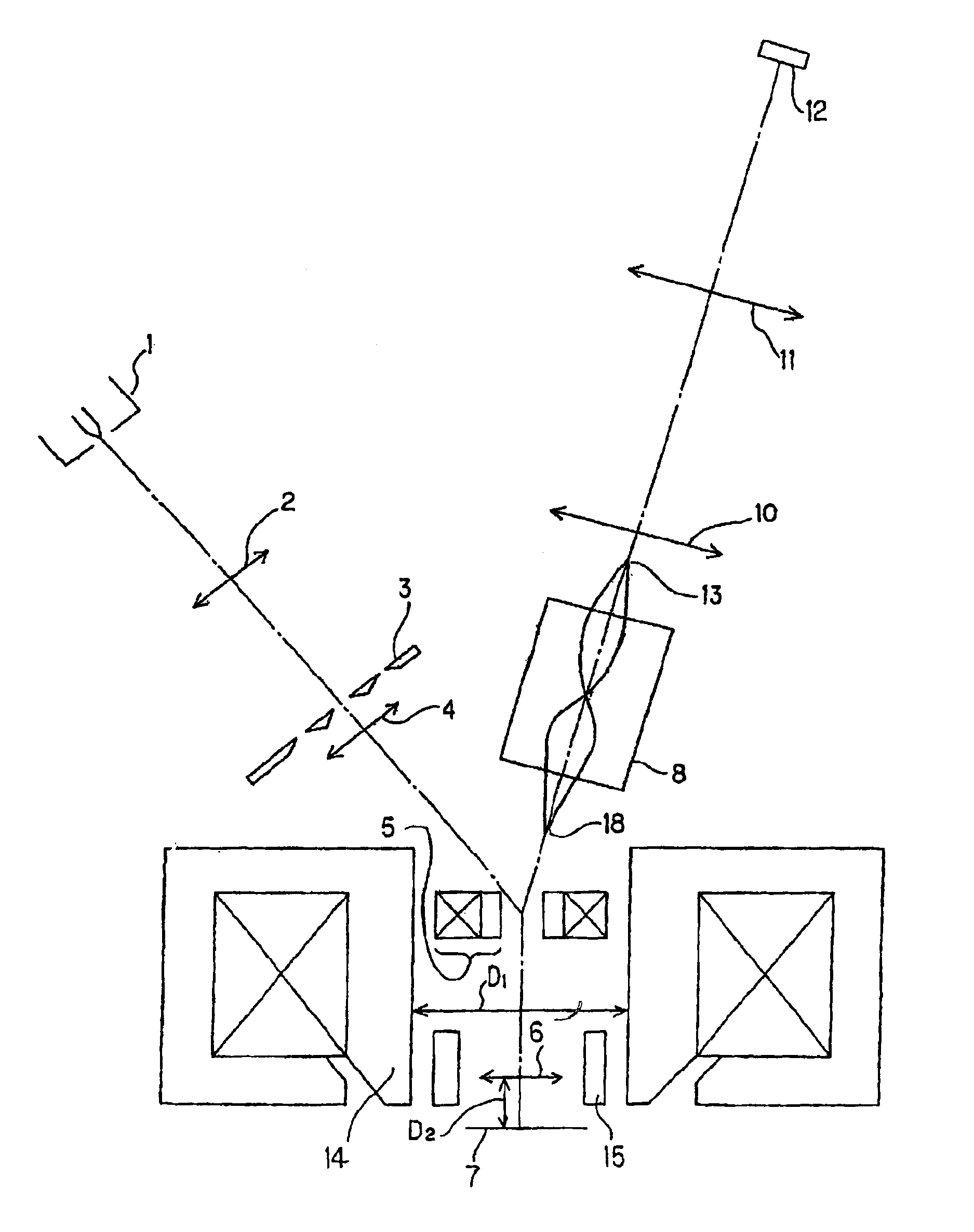
Figure 1 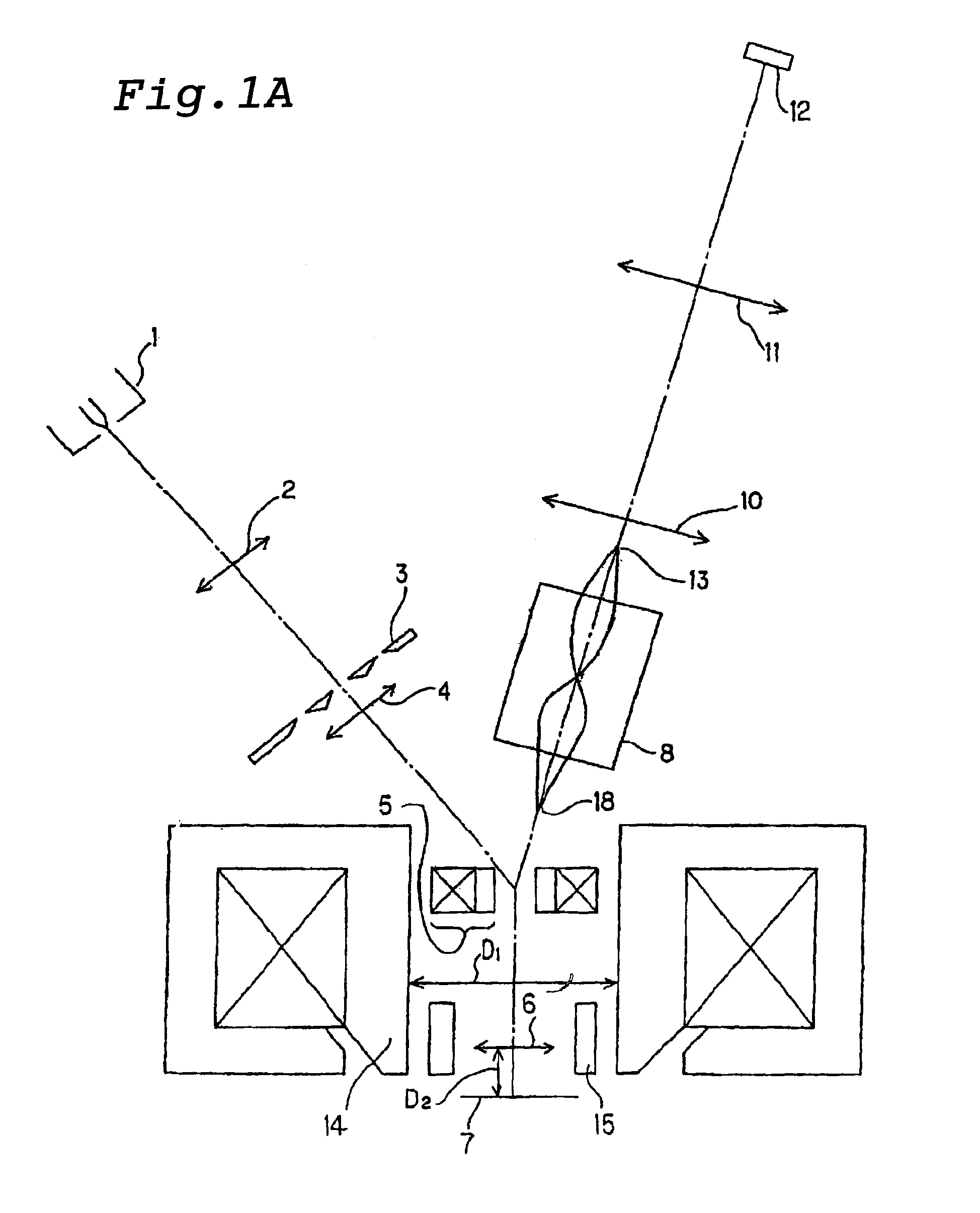
Figure 2 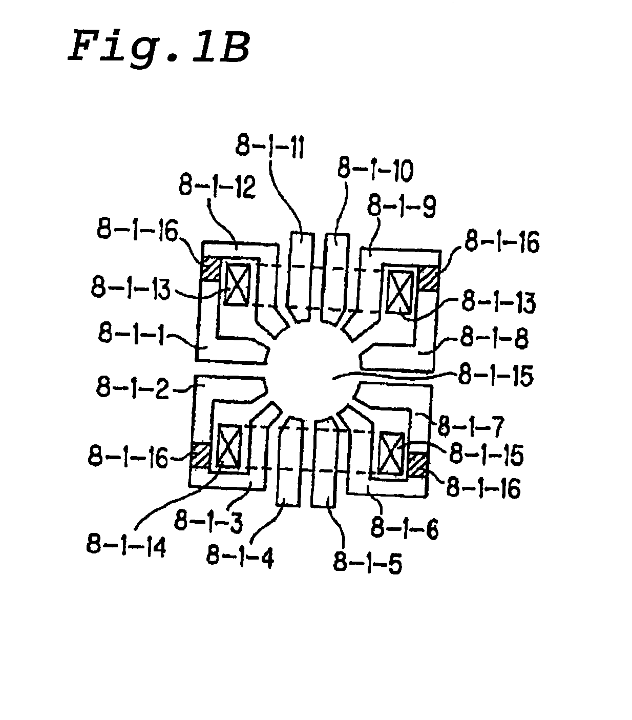
Figure 3
Abstract
Description
CROSS-REFERENCE TO RELATED APPLICATIONS
[0001] This application is a division of U.S. application Ser. No. 11 / 817,763, filed on Dec. 8, 2008 which is based on Japanese Patent Application No. 2004-306641 filed on Oct. 21, 2004 and Japanese Patent Application No. 2005-032157 filed on Feb. 8, 2005, and which is based on and claims priority of Japanese Patent Application No. 2005-059504 filed on Mar. 3, 2005, Japanese Patent Application No. 2005-092297 filed on Mar. 28, 2005, and Japanese Patent Application No. 2005-092314 filed on Mar. 28, 2005, the entire contents of which are incorporated herein by reference.TECHNICAL FIELD
[0002] The present invention relates to a projection electron beam apparatus and a defect inspection system using the apparatus, and more particularly, to an electron beam apparatus which has a projection electro-optical system to have the abilities to conduct a defect inspection and the like for semiconductor wafer and the like at a high throughput, and a defect insp...
Examples
example)
Example )
[0362]Indicated Direction: Right . . . Stage Moving Direction: Left (an image moves to the left=the field of view moves to the right)
[0363]Indicated Direction: Upward . . . Stage Moving Direction: Downward (an image moves downward=the field of view moves upward)
(2) Direct Entry of Coordinates on GUI:
[0364]Coordinates directly entered on the GUI are regarded as a location at which the operator wishes to view on the wafer coordinate system, so that the stage is moved such that the coordinate on a wafer are displayed at the center of a captured image.
[0365]In the apparatus described in connection with FIG. 14, a procedure is taken to mount a correction ring on the electrostatic chuck, and position a wafer such that the wafer fits in the inner diameter of the correction ring. Therefore, in the inspection apparatus illustrated in FIG. 15, a procedure is taken to mount a correction ring on a wafer in the load lock chamber 22•1, integrally transfer the wafer mounted with the corre...