
Multi-layer variable micro structure for sensing substance
a micro structure and multi-layer technology, applied in solid-state devices, instruments, material analysis, etc., can solve the problem of weak raman scattering signal of conventional raman spectroscopy for trace chemical detection, and achieve the effect of enhancing the intensity of scattered ligh
Patent Information
- Authority / Receiving Office
- US · United States
- Patent Type
- Applications(United States)
- Current Assignee / Owner
- Publication Date
- 2012-04-12
- Estimated Expiration
- Not applicable · inactive patent
Smart Images
Figure 1 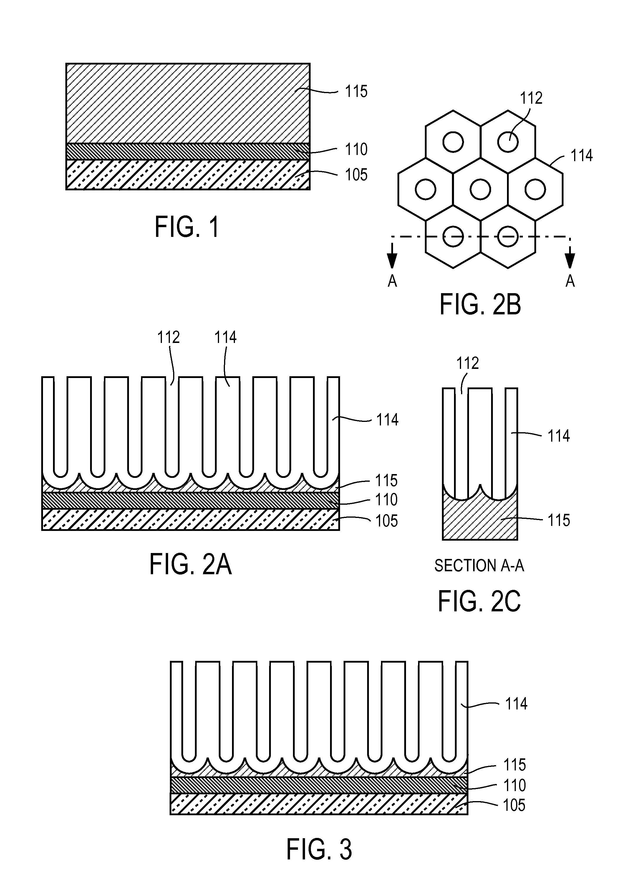
Figure 2 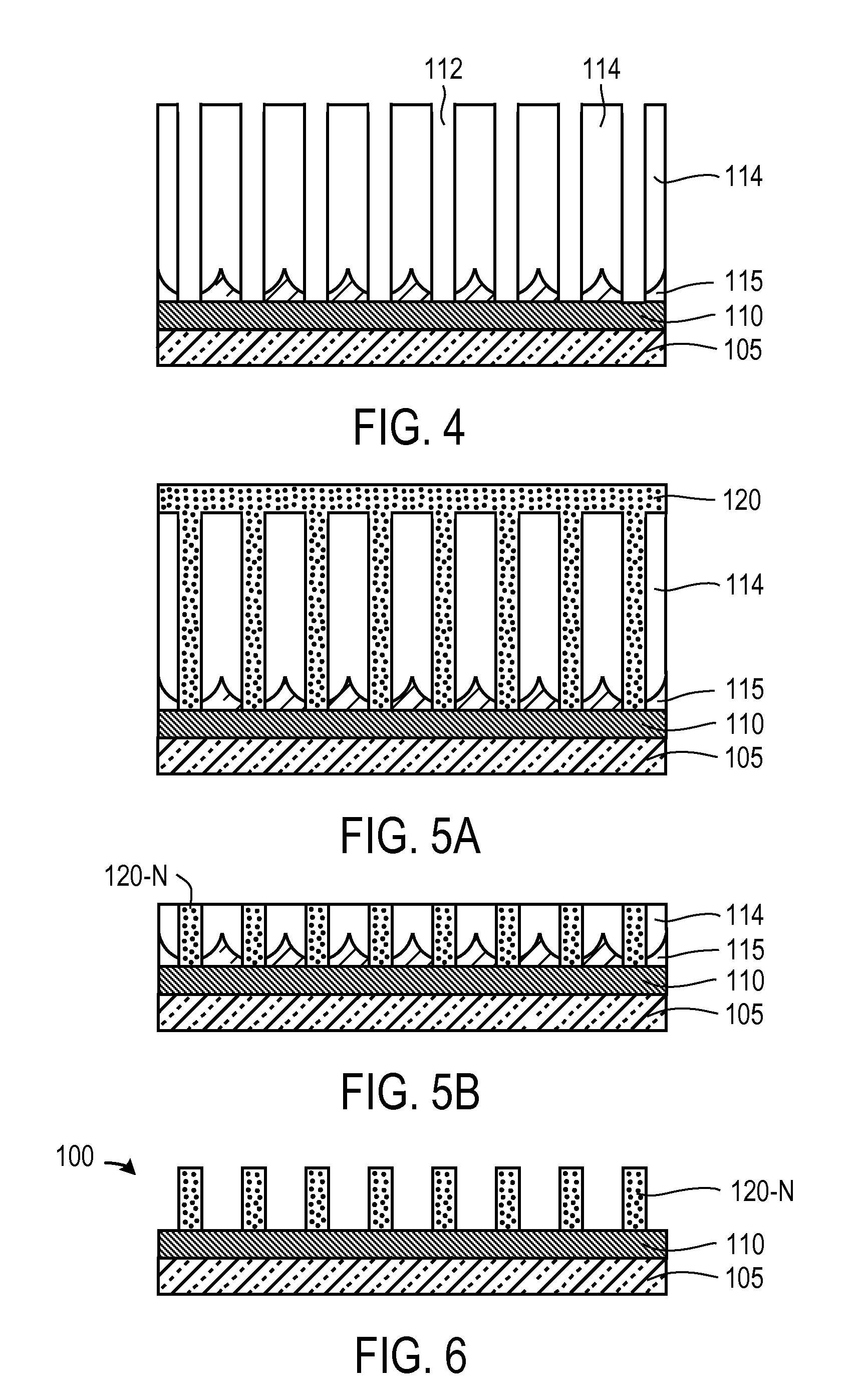
Figure 3
Abstract
Description
[0001] The present patent application is a Continuation-in-Part patent application of and claims priority to commonly assigned copending U.S. patent application Ser. No. 13 / 030,274, entitled “Multi-layer micro structure for sensing substrate” filed Feb. 18, 2011 by the same inventors, which in turns is Continuation-in-Part patent application of and claims priority to commonly assigned copending U.S. patent application Ser. No. 11 / 754,912 (now issued as U.S. Pat. No. 7,892,489), entitled “Light scattering device having multi-layer micro structure” filed May 29, 2007 by the same inventors. The present patent application is also related to commonly assigned copending U.S. patent applications Ser. No. 12 / 643,689 filed Jan 26, 2010 (to be issued as U.S. Pat. No. 8,081,308), Ser. No. 13 / 080,142 filed Apr. 5, 2011, and Ser. No. 12 / 848,893 filed Aug. 2, 2010. The disclosures in the above patent applications are incorporated herein by reference.BACKGROUND OF THE INVENTION
[0002] The present app...
Examples
Embodiment Construction
[0067]Referring to FIGS. 1 to 6 for a series of processing steps to fabricate a nano-structured noble metal surface of this application, FIG. 1 shows a two-layer structure with n-type (100) silicon wafer (3-8 Ω-cm) or oxidized (30-50 nm SiO2) p-type (100) silicon wafers (5-10 mΩ-cm), an electrically and thermally conductive layer 110 deposited on a (100) silicon substrate 105. The thickness of the conductive layer 110, such as Ti and Ni, is optimized to provide i) best adhesion to a subsequently deposited noble metal film, such as Ag, or Au film, etc., ii) electrical conductive film to apply electrical bias to sensing surface in field application, iii) thermal conductive layer to apply lower temperature of sensing surface, iv) thermal heat sink film to conduct localized heat generated by excitation of a light source. The thickness of this metal film is usually controlled in the range of 50 Å-50,000 Å, or 100 Å-1,000 Å. Then an aluminum layer 115 with purity of 99.999% and thickness ...