
Silicon wafers by epitaxial deposition
a technology of silicon wafers and epitaxial deposition, which is applied in the direction of specific components, crystal growth process, polycrystalline material growth, etc., can solve the problems of high cost of silicon wafer manufacturing, and insufficient evidence of cost advantages of most thin film processes. achieve the effect of reducing silicon usage and production cost, high efficiency and reducing manufacturing costs of single crystals
Patent Information
- Authority / Receiving Office
- US · United States
- Patent Type
- Applications(United States)
- Current Assignee / Owner
- Publication Date
- 2013-02-07
- Estimated Expiration
- Not applicable · inactive patent
Smart Images
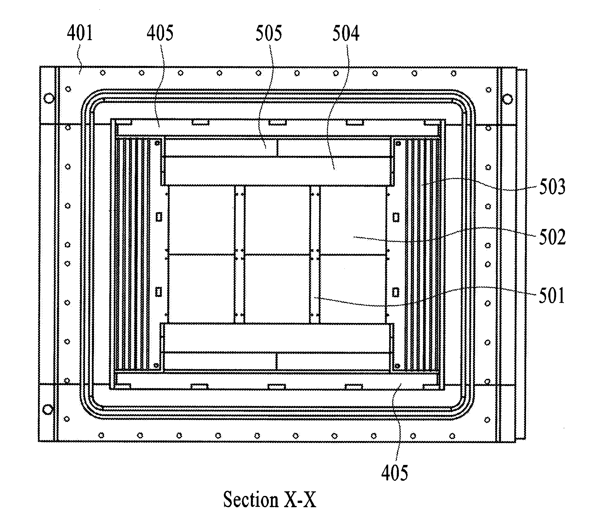
Figure 1 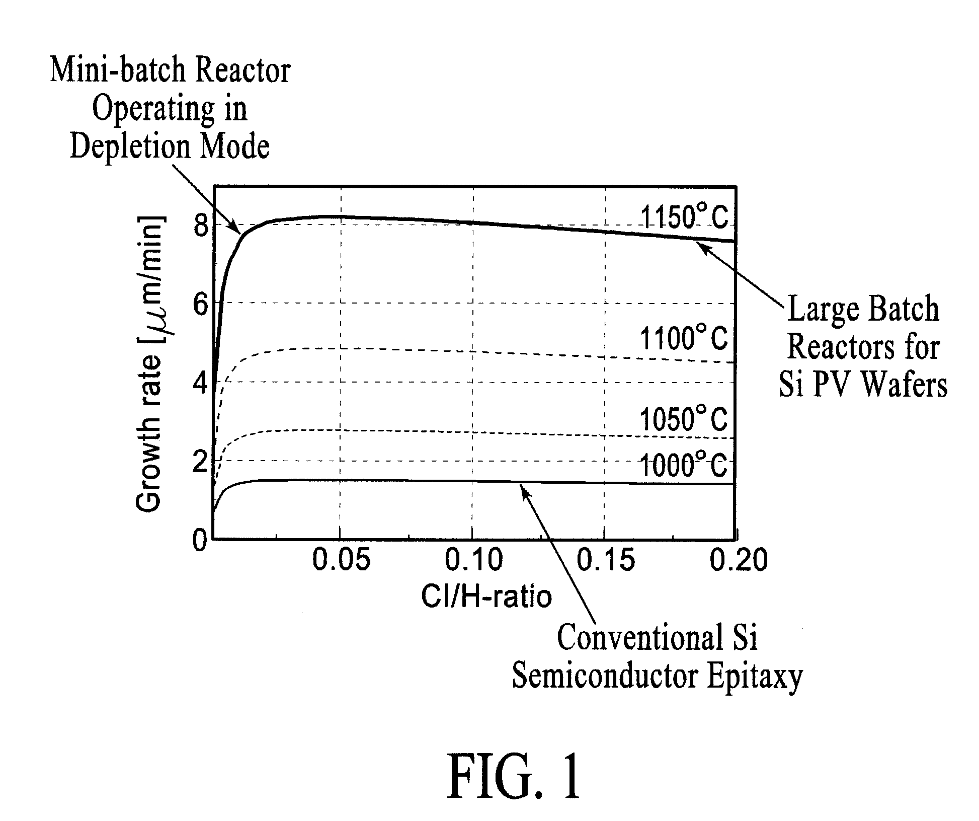
Figure 2 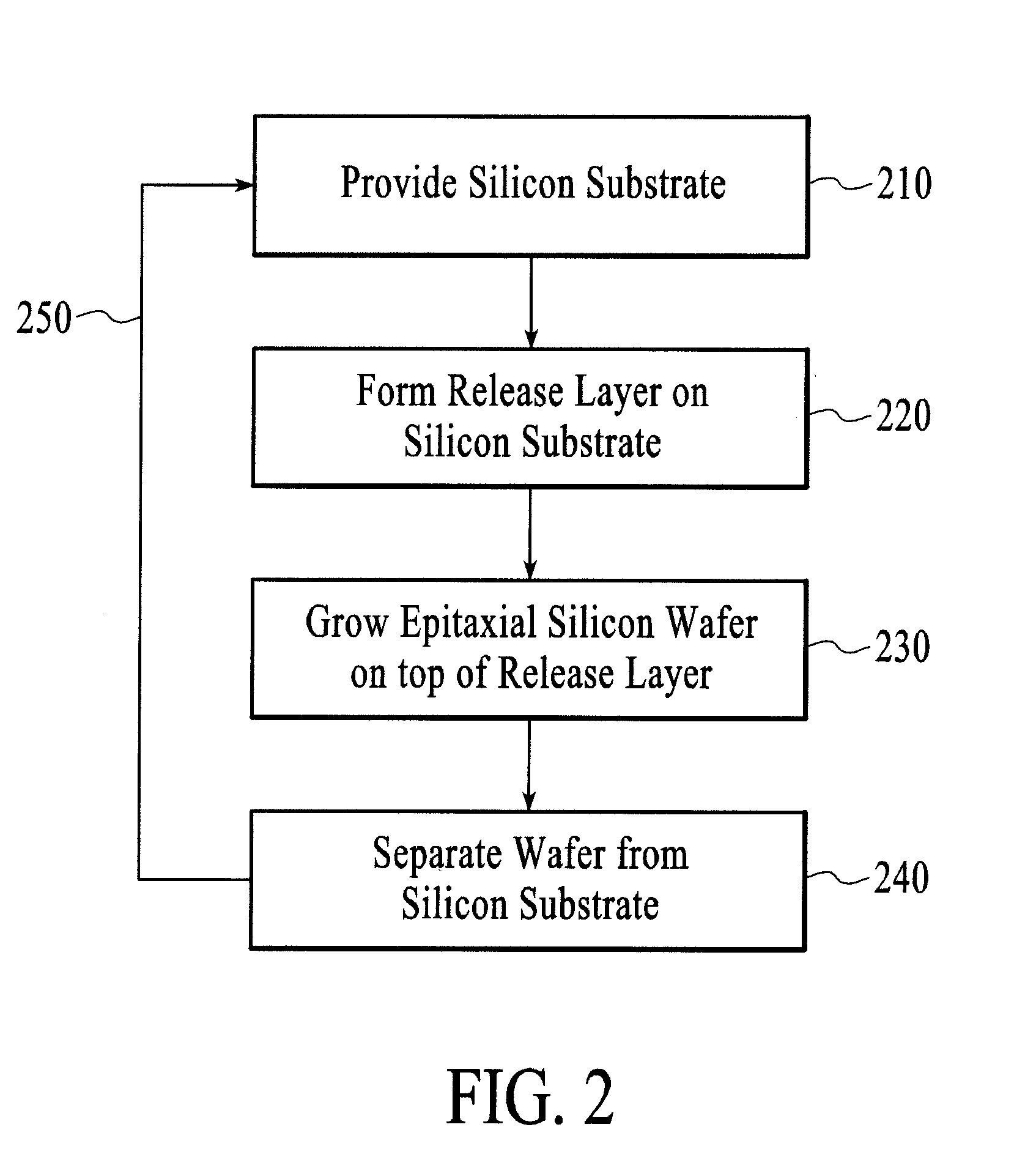
Figure 3
Abstract
Description
CROSS-REFERENCE TO RELATED APPLICATIONS
[0001] This application claims the benefit of U.S. Provisional Application No. 61 / 491,152 filed May 27, 2011, incorporated herein by reference in its entirety.FIELD OF THE INVENTION
[0002] The present invention relates generally to fabrication of silicon wafers, and more particularly to fabrication of silicon wafers by epitaxial deposition.BACKGROUND
[0003] Crystalline silicon provides high solar cell efficiencies, η, of up to approximately 23% in commercial production environments, together with advantages, when compared with thin film solar cells such as CIGS, CdTe, etc., of (a) availability, (b) environmentally friendliness, and (c) demonstrated long lifetimes and associated technology maturity. However, crystalline silicon traditionally has a higher photovoltaic module cost than competitive thin-film panels. (A module is the unit that actually generates power and includes a frame holding a number of solar cells, the latter being electrically con...
Examples
Embodiment Construction
[0053]Embodiments of the present invention will now be described in detail with reference to the drawings, which are provided as illustrative examples of the invention so as to enable those skilled in the art to practice the invention. Notably, the figures and examples below are not meant to limit the scope of the present invention to a single embodiment, but other embodiments are possible by way of interchange of some or all of the described or illustrated elements. Moreover, where certain elements of the present invention can be partially or fully implemented using known components, only those portions of such known components that are necessary for an understanding of the present invention will be described, and detailed descriptions of other portions of such known components will be omitted so as not to obscure the invention. In the present specification, an embodiment showing a singular component should not be considered limiting; rather, the invention is intended to encompass ...