
Thin film transistor array substrate and method for manufacturing the same
Patent Information
- Authority / Receiving Office
- US · United States
- Current Assignee / Owner
- Publication Date
- 2013-08-08
- Estimated Expiration
- Not applicable · inactive patent
Smart Images
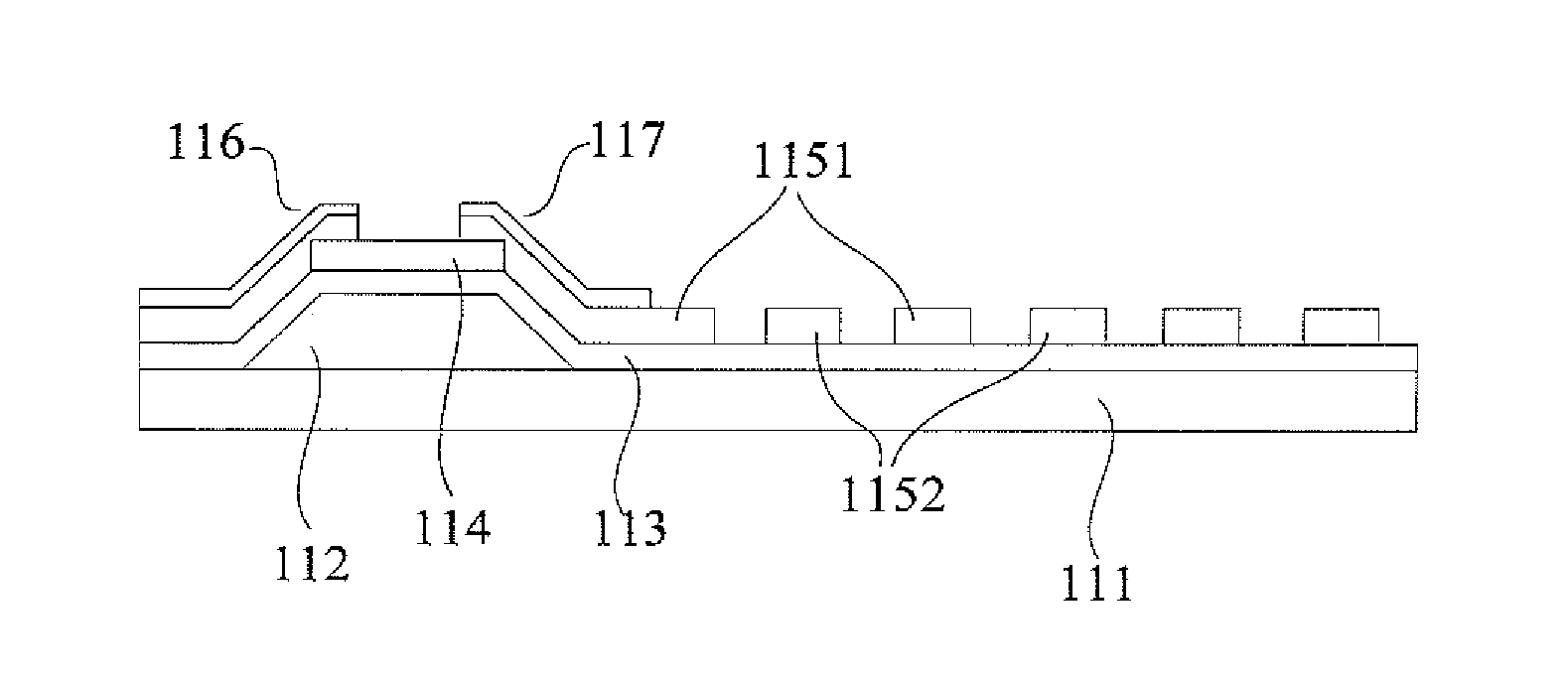
Figure 1 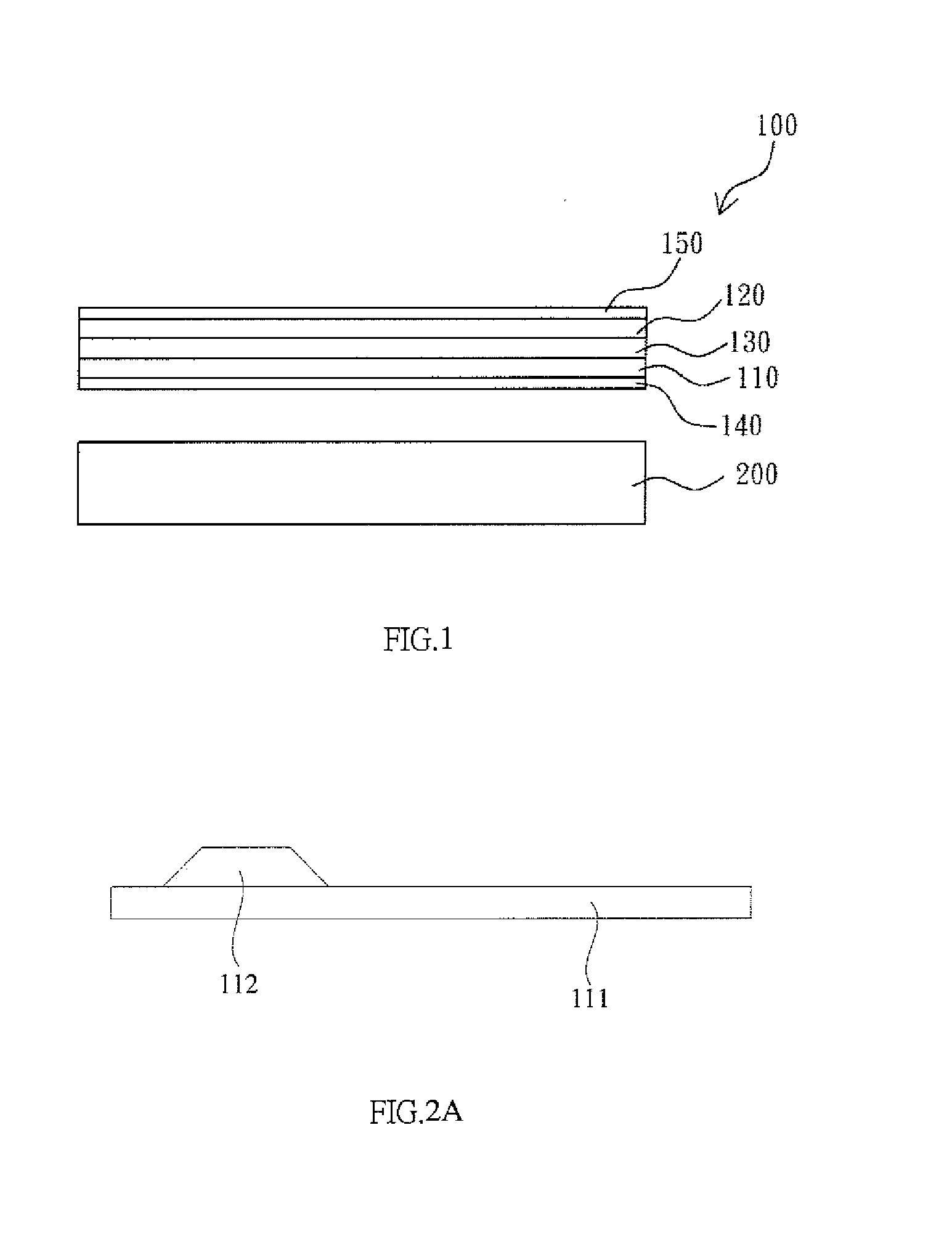
Figure 2 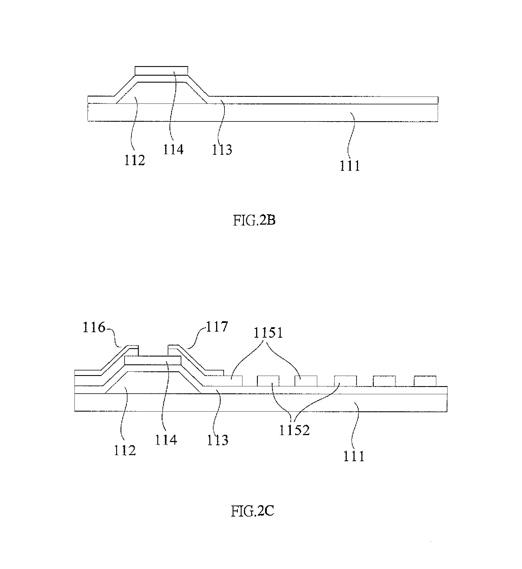
Figure 3
Abstract
Description
FIELD OF THE INVENTION
[0001] The present invention relates to a field of a manufacturing technology for liquid crystal displays (LCDs), and more particularly to a thin film transistor (TFT) array substrate and a method for manufacturing the same.BACKGROUND OF THE INVENTION
[0002] In accordance with a development of LCDs, a high display performance of the LCDs is required. For example, more and more in-plane switching mode (IPS) mode LCDs are applicable to the field of the liquid crystal display technology.
[0003] In a process for fabricating the TFT array substrate of the LCDs, masks are required to execute photolithography processes. However, the masks for photolithography are very expensive. The more the number of the masks is, the higher the cost for fabricating the TFT is. Furthermore, more masks will result in longer process time and more complicated process.
[0004] Similarly, in the conventional technology, it is more complicated to fabricate the TFT array substrate of the IPS mode L...
Examples
Embodiment Construction
[0031]The following embodiments are referring to the accompanying drawings for exemplifying specific performable embodiments of the present invention. Furthermore, directional terms described by the present invention, such as upper, lower, front, back, left, right, inner, outer, side and etc., are only directions by referring to the accompanying drawings, and thus the used directional terms are used to describe and understand the present invention, but the present invention is not limited thereto.
[0032]In the drawings, structure-like elements are labeled with like reference numerals.
[0033]Referring to FIG. 1, a cross-sectional view showing a display panel and a backlight module according to an embodiment of the present invention is illustrated. The method of the present embodiment for manufacturing a TFT array substrate can be applicable to the fabrication of the display panel 100, such as a liquid crystal display panel. When utilizing the display panel 100 of the present embodiment...