
Pixel structure and driving method capable of switching display mode
a driving method and display mode technology, applied in the field of pixel structure, can solve the problems often sacrificed transmittance of pixel structures in display apparatuses, and achieve the effects of shortening the response time of liquid crystals, high transmittance, and high transmittan
Patent Information
- Authority / Receiving Office
- US · United States
- Patent Type
- Applications(United States)
- Current Assignee / Owner
- Publication Date
- 2019-07-25
Smart Images
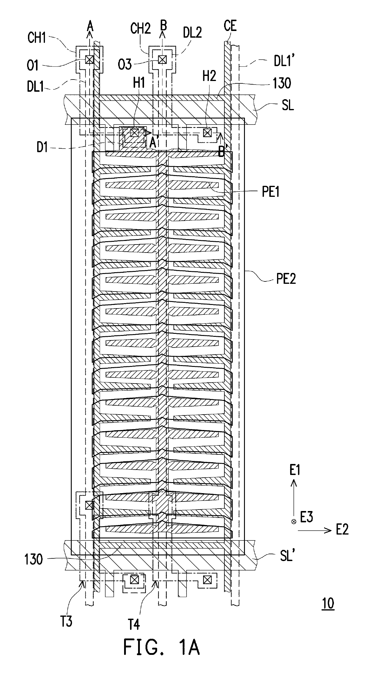
Figure 1 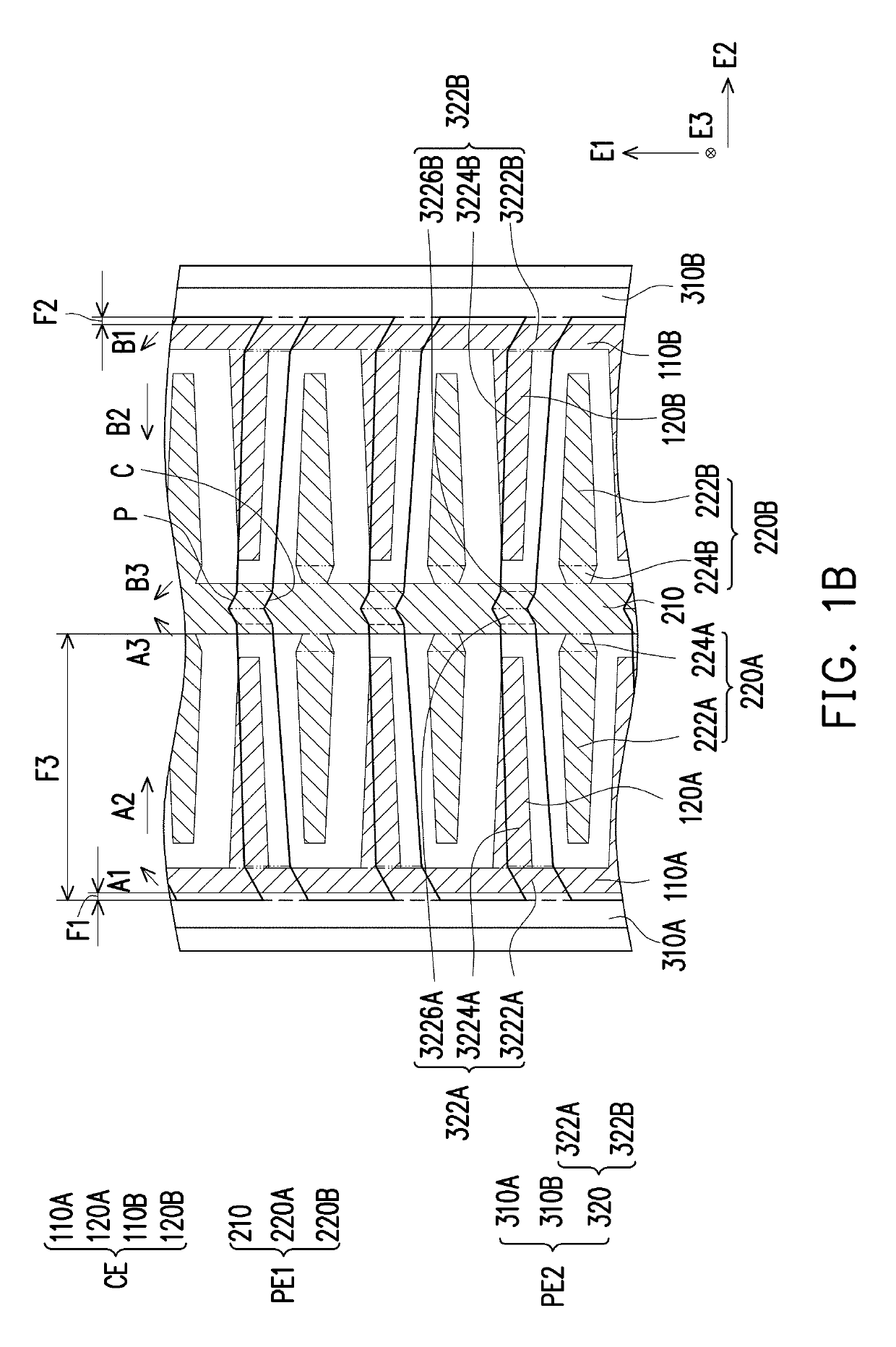
Figure 2 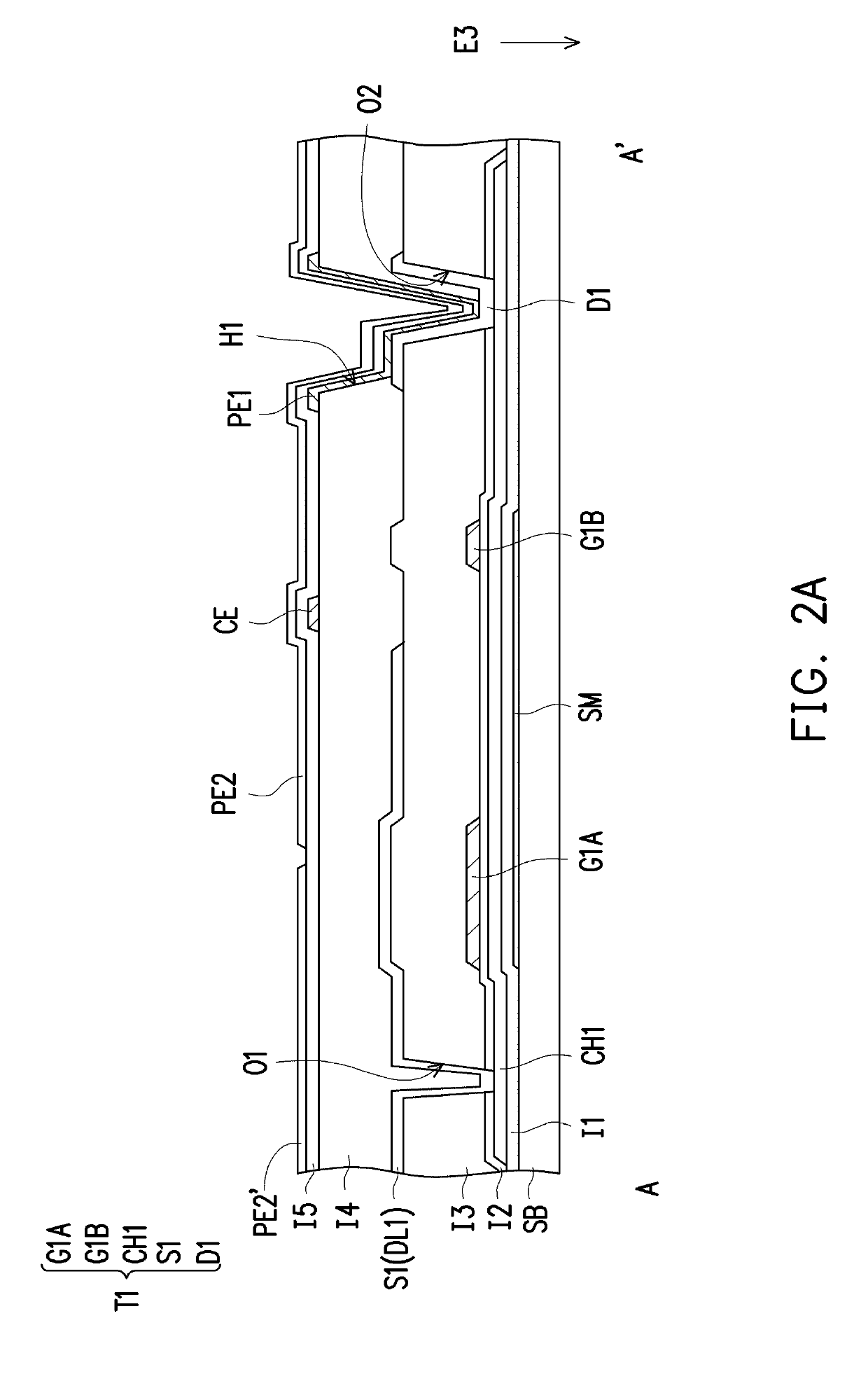
Figure 3
Abstract
Description
CROSS-REFERENCE TO RELATED APPLICATION
[0001] This application claims the priority benefit of Taiwan application serial no. 107102545, filed on Jan. 24, 2018. The entirety of the above-mentioned patent application is hereby incorporated by reference herein and made a part of this specification.BACKGROUND OF THE INVENTIONField of the Invention
[0002] The invention relates to a pixel structure, and particularly relates to a pixel structure having a common electrode, a first electrode and a second electrode, and a driving method capable of switching display modes.Description of Related Art
[0003] With advances in technology, demands for performance of display apparatuses have been gradually increasing, especially virtual reality (VR) display apparatuses, augmented reality (AR) display apparatuses and so on. How to shorten liquid crystal response time is particularly important in order to avoid image delay.
[0004] However, while shortening liquid crystal response time, a light transmittance of ...
Examples
Embodiment Construction
[0028]The invention will have a more comprehensive description hereinafter with reference to the accompanying drawings, in which embodiments of the invention are shown. As those skilled in the art would realize, the described embodiments may be modified in various different ways, without departing from the spirit or scope of the invention.
[0029]The use of “electrically connected” in the text may mean that at least two elements directly contact or indirectly electrically contact with each other. The manner of being indirectly electrically contact with each other is exemplified as the elements are in physical contact or electrical contact with each other via an intermediate element. The aforementioned intermediate element may be a switch (for example, a thin film transistor) or an element such as a resistor or a capacitor. The use of “electrically connected” may also represent that at least two elements operate or act on each other.
[0030]FIG. 1A is a schematic top view of a pixel stru...