
Apparatus for manufacturing an electronic device, method of manufacturing an electronic device, and program for manufacturing an electronic device
Patent Information
- Authority / Receiving Office
- US · United States
- Current Assignee / Owner
- Publication Date
- 2006-03-28
- Estimated Expiration
- Not applicable · inactive patent
Smart Images
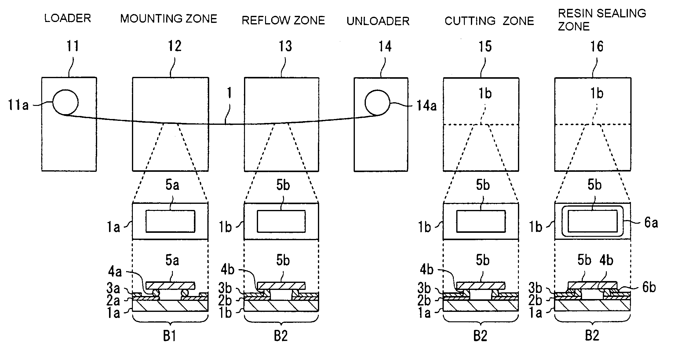
Figure 1 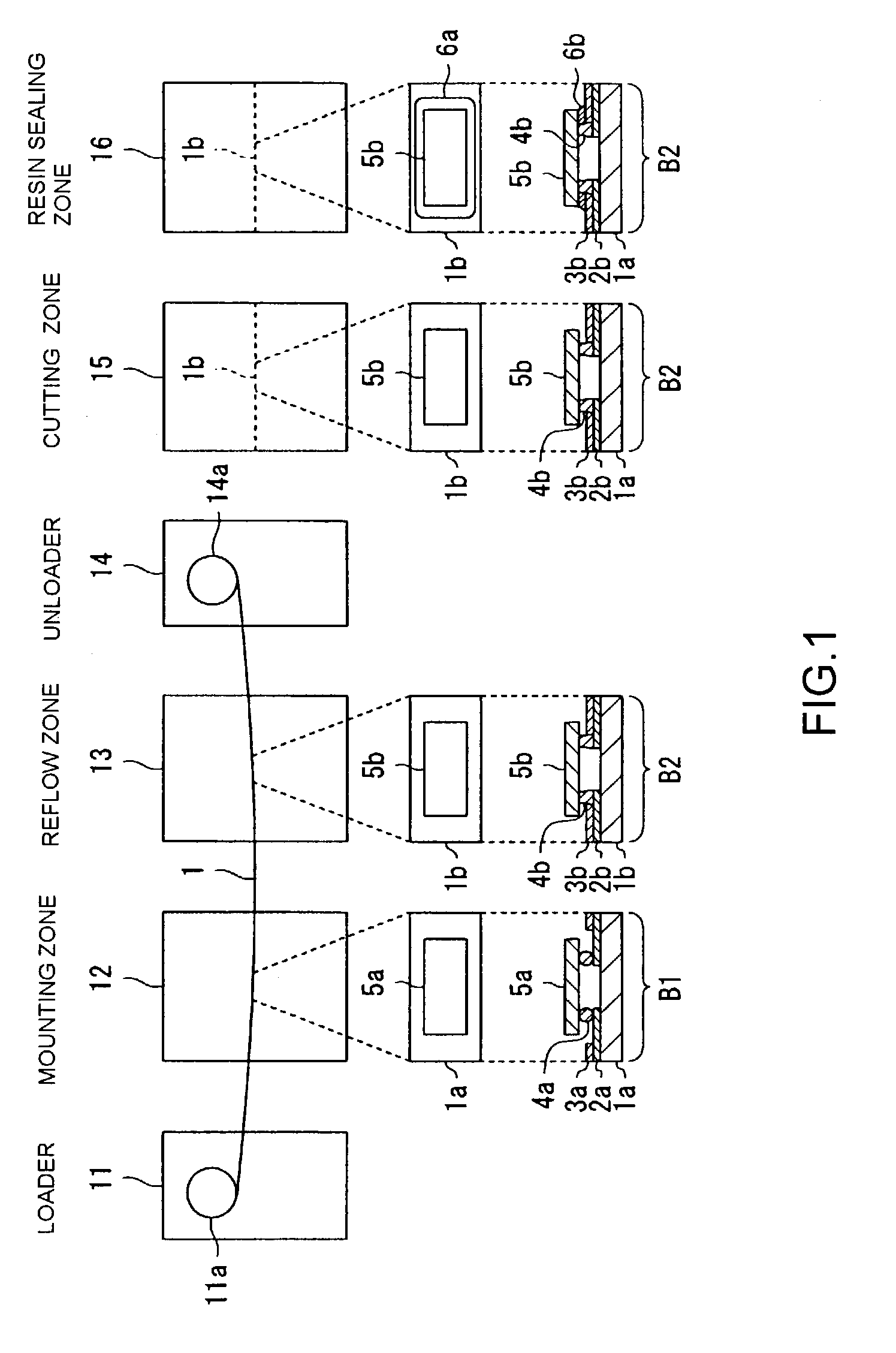
Figure 2 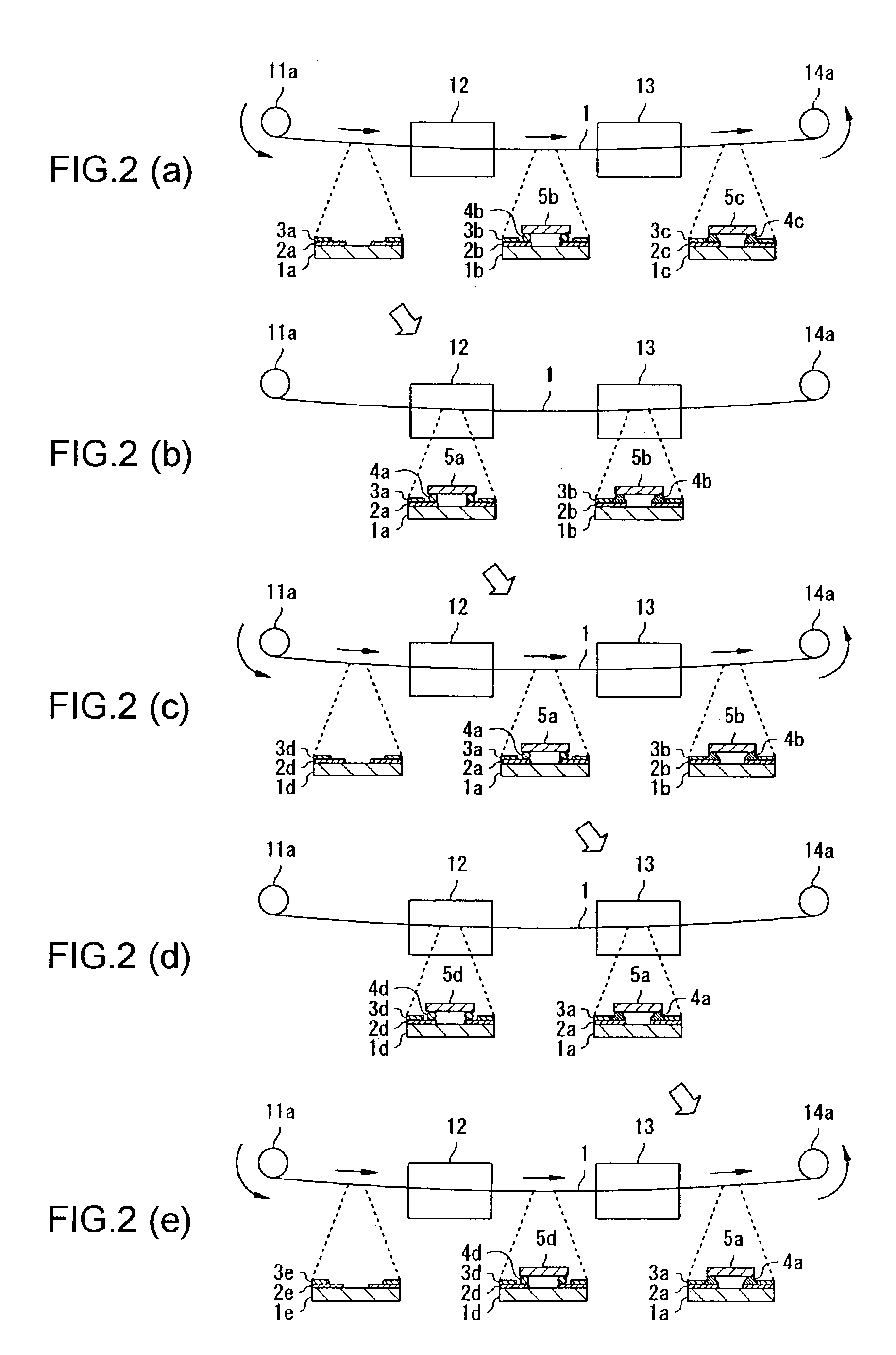
Figure 3
Abstract
Description
BACKGROUND OF THE INVENTION
[0001] 1. Technical Field of the Invention
[0002] The present invention relates to an apparatus, a method, and a program for manufacturing an electronic device, and more particularly to a soldering reflow process for a tape substrate, or the like on which electronic components are mounted.
[0003] 2. Description of the Related Art
[0004] Generally, if semiconductor chips are mounted on a circuit substrate of a COF (Chip On Film) module, a TAB (Tape Automated Bonding) module, or the like in a conventional apparatus for manufacturing an electronic device, a method for performing a soldering / printing treatment, an electronic component mounting treatment, and a reflow treatment in a reel-to-reel method is used.
[0005] FIG. 23 illustrates a conventional method of manufacturing an electronic device. In FIG. 23, a solder applying zone 122 is arranged between a loader 121 and an unloader 123, and a mounting zone 132 between a loader 131 and an unloader 133, and a reflow zon...
Examples
first embodiment
[0175]FIG. 2 is a diagram for illustrating an electronic device manufacturing process according to the present invention;
[0176]In FIG. 2(a), circuit substrates 1a to 1c are formed on the tape substrate 1 retracted between the unwinding reel 11a and a take-up reel 14a. At this time, a wiring 2a and an insulating film 3a are formed on the circuit substrate 1a. A wiring 2b and an insulating film 3b are formed on the circuit substrate 1b, and a semiconductor chip 5b where the soldering material ball 4b is formed is mounted on the circuit substrate 1b, a wiring 2c and an insulating film 3c are formed on the circuit substrate 1c, and a semiconductor chip 5c is fixed via the soldering material ball 4c. Moreover, in the tape substrate 1, with the circuit substrate 1a to 1c retracted, according to a predetermined transport tact, the circuit substrate 1a to which the mounting treatment has not been performed yet is transported to the mounting zone 12, and the circuit substrate 1b to which the...