

Clock control of state storage circuitry
a state storage circuit and clock control technology, applied in the direction of logic circuits, information storage, electronic circuit testing, etc., can solve the problems of slow propagation of data signals into the master stage, increase the clock to output delay, etc., to increase the complexity of clock signal generating circuitry, increase the maximum speed of state storage circuitry, and operate faster
Patent Information
- Authority / Receiving Office
- US · United States
- Patent Type
- Patents(United States)
- Current Assignee / Owner
- Publication Date
- 2011-02-22
Smart Images
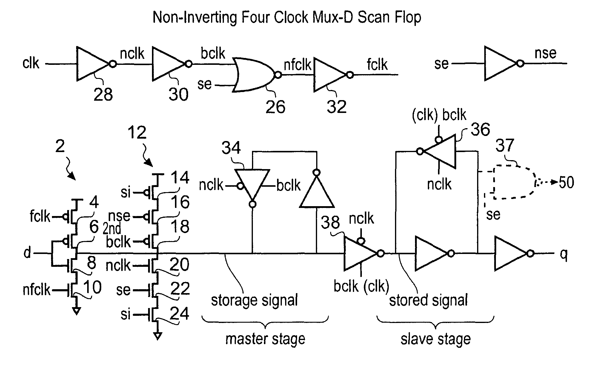
Figure 1 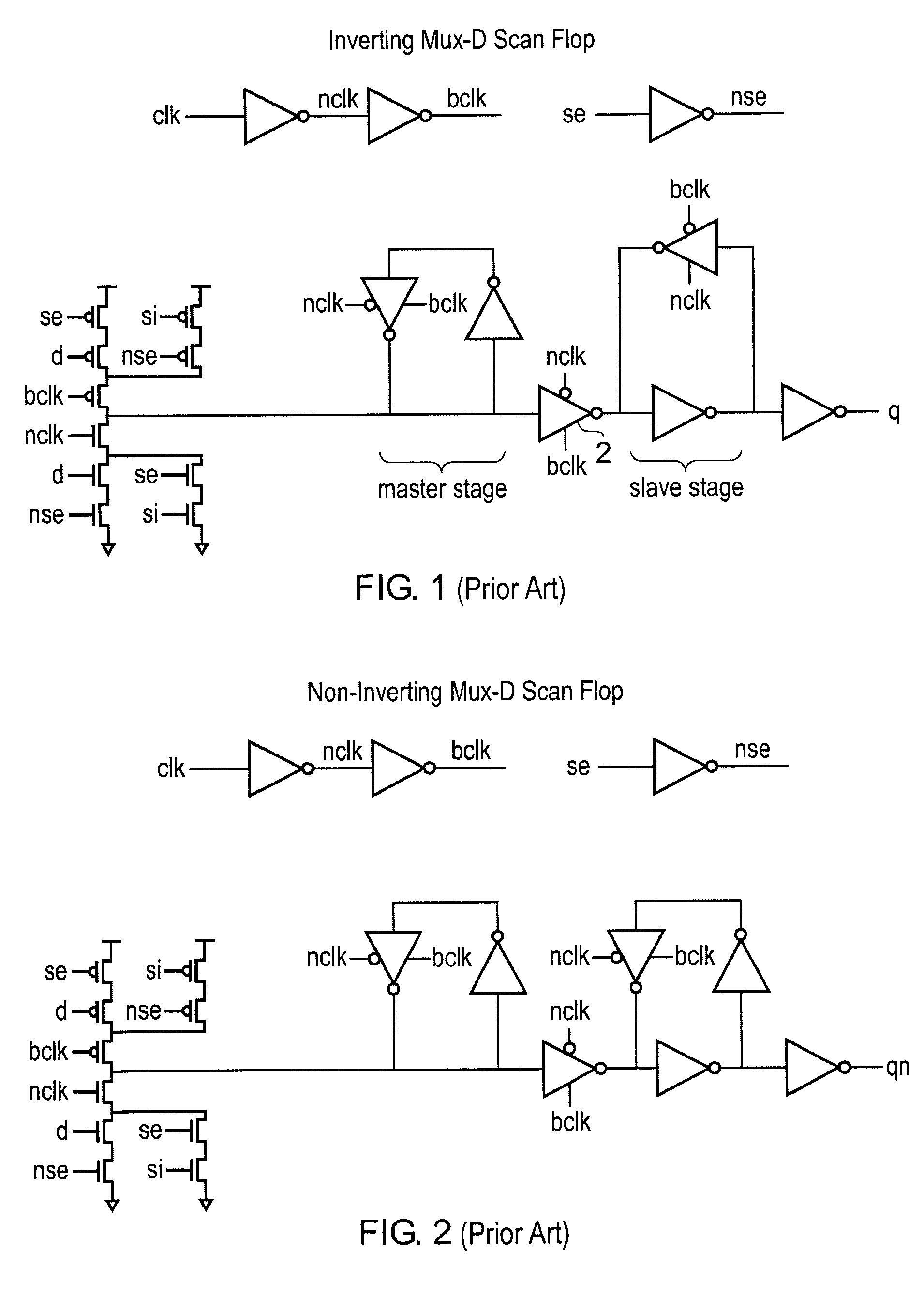
Figure 2 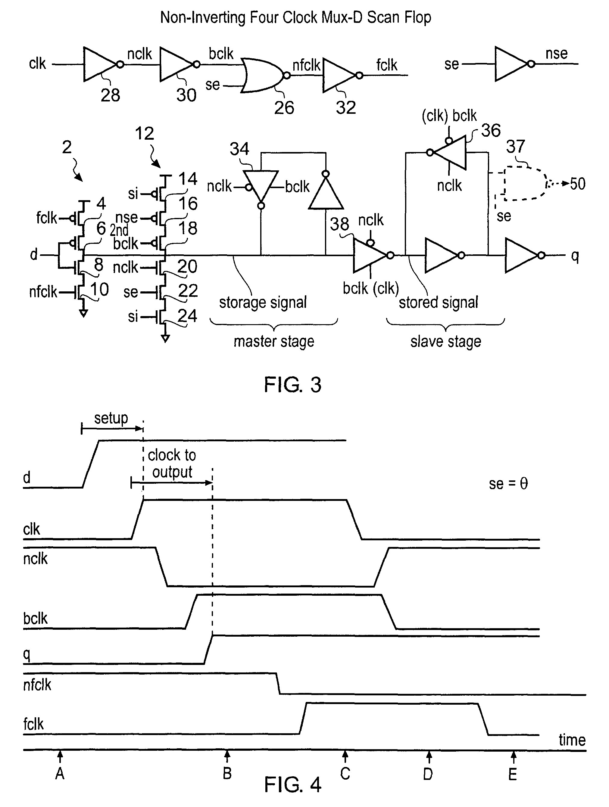
Figure 3
Abstract
Description
BACKGROUND OF THE INVENTION
[0001] 1. Field of the Invention
[0002] This invention relates to the field of state storage circuitry, including different types of latches, flip-flops, registers etc. More particularly, this invention relates to the control of such state storage circuitry with clock signals.
[0003] 2. Description of the Prior Art
[0004] FIG. 1 of the accompanying drawings illustrates a known inverting mux-D scan flop built using CMOS circuitry. The functional data signal d is applied to a P-type gate and a N-type gate within a stack comprising three P-type gates and three N-type gates. This stack also includes two gates switched by the scan enable signal se and the complement of the scan enable signal nse. The final two transistors within the stack are switched by the complement nclk of the input clock clk to the clock tree illustrated as well as a buffered clock bclk generated from clock nclk. When scan enable is not asserted, the gates controlled by the scan enable signal se ...
Examples
Embodiment Construction
[0037]FIG. 3 shows tristate logic circuitry in the form of tristate inverter circuitry 2 comprising two P-type gates 4, 6 and two N-type gates 8, 10. The output from this tristate inverting circuitry 2 drives the storage signal which is applied to the master stage of the state storage circuitry. Tristate scan signal insertion circuitry 12 comprises three P-type gates 14, 16, 18 and three N-type gates 20, 22, 24. The tristate scan signal insertion circuitry 12 drives the storage signal during scan mode.
[0038]In functional mode the scan enable signal se is not asserted (low) and accordingly gates 22 and 16 are switched off and the tristate scan signal insertion circuitry 12 is tristated and not driving the storage signal. During the scan mode the tristate scan signal insertion circuitry 12 does drive the storage signal and in this case the clock signals to the gates 4 and 10 respectively comprising the fourth clock signal fclk and the third clock signal nfclk are held at fixed values ...