
Film forming apparatus and film forming method
a metal film and film forming technology, applied in the direction of electrolysis process, semiconductor devices, electrolysis components, etc., can solve the problems of uneven thickness of metal film, impeded current flow from the location where oxygen gas has accumulated (i.e., a part of the surface of the anode) toward the cathode, etc., and achieve the effect of few defects
Patent Information
- Authority / Receiving Office
- US · United States
- Patent Type
- Patents(United States)
- Current Assignee / Owner
- Publication Date
- 2017-09-05
Smart Images
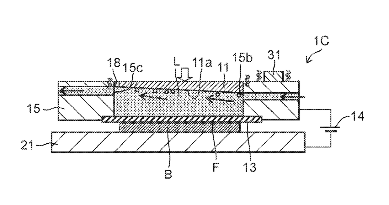
Figure 1 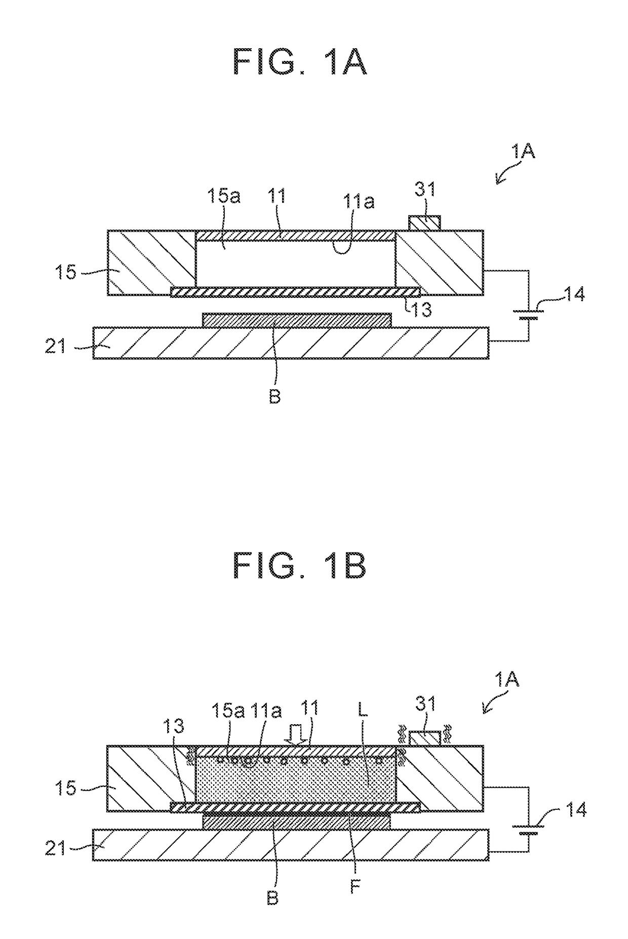
Figure 2 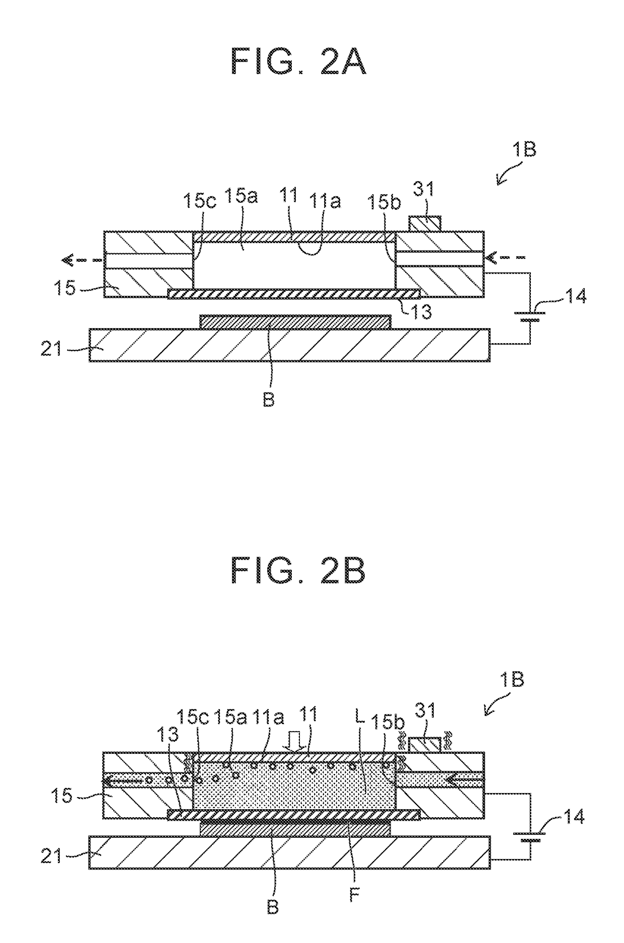
Figure 3
Abstract
Description
INCORPORATION BY REFERENCE
[0001] The disclosure of Japanese Patent Application No. 2015-048021 filed on Mar. 11, 2015 including the specification, drawings and abstract is incorporated herein by reference in its entirety.BACKGROUND OF THE INVENTION
[0002] 1. Field of the Invention
[0003] The invention relates to a metal-film forming apparatus and a metal-film forming method capable of suitably forming a metal film by applying voltage between an anode and substrate, and depositing metal from metal ions contained in a solid electrolyte membrane onto a surface of the substrate.
[0004] 2. Description of Related Art
[0005] Conventionally, when manufacturing an electronic circuit substrate or the like, a nickel film is formed on a surface of a substrate in order to form a nickel circuit pattern. As film forming technology of such a metal film, technology that forms a metal film by a plating process such as a non-electrolytic plating process, or that forms a metal film by a PVD method such as sputt...
Examples
Embodiment Construction
[0055]Hereinafter, a film forming apparatus capable of suitably carrying out a metal-film forming method according to example embodiments of the invention will be described.
[0056]FIGS. 1A and 1B are conceptual diagrams showing frame formats of a film forming apparatus 1A for forming a metal film F according to a first example embodiment of the invention. FIG. 1A is a sectional view showing a frame format of a state of the film forming apparatus 1A before forming a film, and FIG. 1B is a sectional view showing a frame format of a state of the film forming apparatus 1A when a film is being formed.
[0057]As shown in FIGS. 1A and 1B, the film forming apparatus 1A is an apparatus that deposits metal from metal ions, and forms a metal film from the deposited metal on a surface of a substrate B. Here, a substrate made of metal material such as aluminum, or a substrate formed by forming a metal base layer on a treated surface of a resin or silicon substrate, may be used as the substrate B.
[0...