
Interface engineering method for perovskite solar cell, and inverted perovskite solar cell and preparation method therefor
By setting a metal oxide nanoparticle layer between the transparent conductive thin film glass layer and the hole transport layer, flattening the TCO surface, and setting an island-shaped nanoparticle layer between the hole transport layer and the perovskite absorbing layer, the wetting ability of the self-assembled single-molecule hole transport layer is improved, and the problem of poor surface wetting ability of the self-assembled single-molecule hole transport layer is solved, and the photoelectric conversion efficiency of perovskite solar cells is improved.
Patent Information
- Application Number
- PCT/CN2024/140157
- Authority / Receiving Office
- WO · WO
- Patent Type
- Applications
- Current Assignee / Owner
- Priority Date
- 2023-12-26
- Filing Date
- 2024-12-18
- Publication Date
- 2025-07-03
AI Technical Summary
In the prior art, the surface wetting of the self-assembled single-molecule hole transport layer is poor, which makes it difficult for perovskite solution to spread rapidly, and the self-assembled single-molecule hole transport layer is unevenly arranged on the rough TCO substrate, affecting the photoelectric conversion efficiency of the battery.
A first metal oxide nanoparticle layer is arranged between the transparent conductive thin film glass layer and the hole transport layer, and fills the glass layer pit to flatten the surface; a second metal oxide nanoparticle layer is arranged between the hole transport layer and the perovskite absorbing layer, forming an island-like covering to improve wetting.
It improves the uniformity of the hole transport layer and the coverage of the perovskite absorbing layer, improves the photoelectric conversion efficiency of perovskite solar cells, and simplifies operations, with good industrial application prospects.
Smart Images
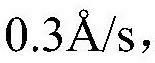
Figure PCTCN2024140157-FTAPPB-I100001 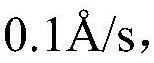
Figure PCTCN2024140157-FTAPPB-I100002 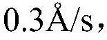
Figure PCTCN2024140157-FTAPPB-I100003
Abstract
Description
Interface control method of perovskite solar cell and inverse perovskite solar cell and preparation method thereof Technical Field
[0001] The present invention relates to an interface control method of a perovskite solar cell and an inverted perovskite solar cell and a preparation method thereof, belonging to the technical field of perovskite solar cells. Background Art
[0002] Perovskite solar cells are a new type of photovoltaic material with the advantages of high efficiency, low cost and adjustable band gap. After more than ten years of rapid development, the efficiency of perovskite single-junction cells has exceeded 26%, and the efficiency of crystalline silicon / perovskite tandem cells based on wide-bandgap perovskites has reached 33.9%.
[0003] The basic structure of perovskite solar cells is a multilayer structure, including the formal nip structure and the trans pin structure. The trans structure has attracted extensive attention and research from academia and industry due to its advantages such as simple preparation process, low-temperature preparation, low hysteresis coefficient, and compatibility with stacked cell structures. The structure of an inverted perovskite solar cell is generally: transparent conductive film (TCO) glass layer / hole transport layer / perovskite light absorption layer / electron transport layer / electrode. Currently, high-efficiency perovskite cells are based on ~0.1cm 2 Small-area devices are prepared by solution spin coating. Industrial-grade perovskite solar cell components are coated with perovskite solution on the hole transport layer using a slit coater.
[0004] Self-assembled monolayers are ordered arrays of organic molecules. In recent years, they have become a commonly used hole transport layer for high-efficiency perovskite single-junction and stacked cells. The anchoring groups in them bind to the substrate, and the top functional groups regulate the surface properties, which together play a role in efficient hole transport.
[0005] The self-assembled monolayer is a kind of self-assembled monolayer, which is a kind of self-assembled monolayer composed of poly (bis (4-phenyl) (2,4,6-trimethylphenyl) amine) (PTAA), nickel oxide (NiO x ) after the new generation of trans-device hole transport layer. Due to the small molecule monolayer structure, the hole extraction and transport efficiency is improved through the charge tunneling effect. The surface wettability of the self-assembled monolayer is a key parameter affecting the subsequent perovskite film formation, especially when the perovskite cell area is enlarged. However, the functional groups on the surface of the self-assembled monolayer often lead to poor wettability of the perovskite film. In addition, due to the single-molecule anchored assembly, the morphology of the resulting hole transport layer depends on the state of the TCO substrate. The commonly used TCO substrate has a large roughness (about 10-100nm), which leads to poor flatness of the self-assembled monomolecule hole transport layer and disordered molecular orientation, which affects the uniformity of charge transfer.
[0006] Al-Ashouri et al. introduced a second component containing a hydrophilic group into the monomolecular hole transport layer to improve the surface wettability of the hole transport layer, such as 1,6-diphosphohexane (Amran Al-Ashouri, et al. Wettability Improvement of a Carbazole-Based Hole-Selective Monolayer for Reproducible Perovskite Solar Cells, ACS Energy Letters, 2023, 8(2), 898-900), but this would reduce the monomolecular anchoring sites and reduce the hole transport ability. There is also a prior art approach to improve the surface wettability of monolayer hole transport layers by modifying organic monolayers with hydrophobic carbazole head groups (M. Liu, A.K. Jen, et al. Defect-Passivating and Stable Benzothiophene-Based Self-Assembled Monolayer for High-Performance Inverted Perovskite Solar Cells. Adv. Energy Mater. 2024, 14, 2303742). However, the molecular structure modification process is complex and the prospects for industrial application are limited. Few prior art reports address the issue of TCO substrate surface roughness affecting the growth and arrangement of self-assembled monolayer hole transport layers.
[0007] Currently, the existing technology still has the following two technical problems. First, the surface wettability of the self-assembled monomolecular hole transport layer is poor, making it difficult for the perovskite solution to spread quickly and naturally, resulting in incomplete coverage of the perovskite light-absorbing layer, causing battery leakage and reducing the battery's photoelectric conversion efficiency. Second, the self-assembled monomolecular hole transport layer is anchored on the rough and undulating TCO substrate, resulting in the accumulation of the organic monolayer in the substrate valleys and the thinning of the organic monolayer in the substrate protrusions, ultimately affecting the hole transport efficiency and the battery's photoelectric conversion efficiency. Summary of the Invention
[0008] To solve the above technical problems, the present invention aims to provide a method for controlling the interface of a perovskite solar cell. The interface control method provided by the present invention can improve the surface wettability of the hole transport layer and improve the arrangement uniformity of the hole transport layer.
[0009] Another object of the present invention is to provide an inverse perovskite solar cell and a method for preparing the same. The inverse perovskite solar cell provided by the present invention has high photoelectric conversion efficiency.
[0010] In order to achieve the above objectives, the first aspect of the present invention provides a method for controlling the interface of a perovskite solar cell, which comprises the following steps:
[0011] Disposing a first metal oxide nanoparticle layer between the hole transport layer and the transparent conductive film (TCO) glass layer;
[0012] Disposing a second metal oxide nanoparticle layer between the hole transport layer and the perovskite light absorbing layer;
[0013] The first metal oxide nanoparticle layer includes first metal oxide nanoparticles, and the first metal oxide nanoparticles include one or a combination of indium tin oxide (ITO) nanoparticles, fluorine-doped tin oxide (FTO) nanoparticles, and nickel oxide (NiO) nanoparticles;
[0014] The second metal oxide nanoparticle layer includes second metal oxide nanoparticles, and the second metal oxide nanoparticles include aluminum oxide (Al 2 O 3 ) nanoparticles and / or aluminum-doped zinc oxide (AZO) nanoparticles.
[0015] In the above-mentioned method for controlling the interface of a perovskite solar cell, preferably, the particle size of the first metal oxide nanoparticles is 30 nm or less, with an average particle size of 1-20 nm. More preferably, the particle size of the first metal oxide nanoparticles is smaller than the surface roughness of the transparent conductive thin film glass layer.
[0016] In the above-mentioned interface control method of perovskite solar cells, preferably, the first metal oxide nanoparticle layer fills the surface pits of the transparent conductive film glass layer, and the filling depth of the first metal oxide nanoparticle layer is about 10-100 nm.
[0017] In the above-mentioned interface control method for perovskite solar cells, preferably, the particle size of the second metal oxide nanoparticles is less than half the thickness of the perovskite light-absorbing layer. More preferably, the particle size of the second metal oxide nanoparticles is 50-100 nm.
[0018] In the above-mentioned interface control method for perovskite solar cells, preferably, the thickness of the highest point of the second metal oxide nanoparticle layer is 50-250 nm.
[0019] In the above-mentioned interface control method for perovskite solar cells, preferably, the surface roughness of the transparent conductive thin film glass layer is 10-100 nm.
[0020] In the above-mentioned interface regulation method of perovskite solar cells, preferably, the hole transport layer is a self-assembled monomolecular hole transport layer.
[0021] In the above-mentioned interface control method for perovskite solar cells, preferably, the thickness of the hole transport layer is a monolayer molecular thickness (<1 nm).
[0022] In the above-mentioned interface control method for perovskite solar cells, preferably, the thickness of the perovskite light-absorbing layer is 400-1200 nm.
[0023] The present invention sets a first metal oxide nanoparticle layer between the hole transport layer and the transparent conductive film (TCO) glass layer, and the first metal oxide nanoparticles are metal oxide nanoparticles with conductive ability and particle size less than the surface roughness of the TCO glass layer, which fills the surface pits of the transparent conductive film glass layer, reduces the roughness of the TCO glass layer, and smoothes the surface of the TCO film, which is conducive to the orderly growth of the self-assembled monomolecular hole transport layer and makes it uniformly arranged. In addition, the present invention sets a second metal oxide nanoparticle layer between the hole transport layer and the perovskite light absorbing layer, and the second metal oxide nanoparticles are metal oxide nanoparticles with low conductivity, which form discontinuous island coverage between them, improve the surface wettability of the self-assembled monomolecular hole transport layer, and improve the coverage of the perovskite light absorbing layer. Therefore, the present invention ultimately improves the photoelectric conversion efficiency of the perovskite solar cell. The interface regulation method of the perovskite solar cell of the present invention is applicable to perovskite single junction or tandem solar cells, such as inverted perovskite solar cells, silicon / perovskite tandem solar cells and full perovskite tandem solar cells.
[0024] The second aspect of the present invention provides an inverted perovskite solar cell, which comprises, from bottom to top, a transparent conductive film (TCO) glass layer, a first metal oxide nanoparticle layer, a hole transport layer, a second metal oxide nanoparticle layer, a perovskite light absorbing layer, an electron transport layer, and an electrode;
[0025] The first metal oxide nanoparticle layer includes first metal oxide nanoparticles, and the first metal oxide nanoparticles include one or a combination of indium tin oxide (ITO) nanoparticles, fluorine-doped tin oxide (FTO) nanoparticles, and nickel oxide (NiO) nanoparticles;
[0026] The second metal oxide nanoparticle layer includes second metal oxide nanoparticles, and the second metal oxide nanoparticles include aluminum oxide (Al 2 O 3 ) nanoparticles and / or aluminum-doped zinc oxide (AZO) nanoparticles.
[0027] In the above-mentioned inverse perovskite solar cell, preferably, the particle size of the first metal oxide nanoparticles is less than 30 nm, and the average particle size is 1-20 nm. More preferably, the particle size of the first metal oxide nanoparticles is smaller than the surface roughness of the transparent conductive thin film glass layer.
[0028] In the above-mentioned inverted perovskite solar cell, preferably, the first metal oxide nanoparticle layer fills the surface pits of the transparent conductive thin film glass layer, and the filling depth of the first metal oxide nanoparticle layer is about 10-100 nm.
[0029] In the above-mentioned inverse perovskite solar cell, preferably, the particle size of the second metal oxide nanoparticles is less than half the thickness of the perovskite light absorbing layer. More preferably, the particle size of the second metal oxide nanoparticles is 50-100 nm.
[0030] In the above-mentioned inverse perovskite solar cell, preferably, the thickness of the second metal oxide nanoparticle layer at its highest point is 50-250 nm.
[0031] In the above-mentioned inverse perovskite solar cell, preferably, the surface roughness of the transparent conductive thin film glass layer is 10-100 nm.
[0032] In the above-mentioned inverse perovskite solar cell, preferably, the hole transport layer is a self-assembled monomolecular hole transport layer.
[0033] In the above-mentioned inverse perovskite solar cell, preferably, the hole transport layer has a thickness of a monolayer molecule (<1 nm).
[0034] In the above-mentioned inverse perovskite solar cell, preferably, the thickness of the perovskite light-absorbing layer is 400-1200 nm.
[0035] In the above-mentioned inverse perovskite solar cell, preferably, the thickness of the electron transport layer is 10-30 nm.
[0036] According to a specific embodiment of the present invention, preferably, the inverse perovskite solar cell further includes: a hole blocking layer, which is arranged between the electron transport layer and the electrode.
[0037] In the above-mentioned inverse perovskite solar cell, preferably, the hole blocking layer has a thickness of 4-8 nm.
[0038] In the above-mentioned inverse perovskite solar cell, preferably, the thickness of the electrode is 50-200 nm.
[0039] A third aspect of the present invention provides a method for preparing the above-mentioned inverse perovskite solar cell, which comprises the following steps:
[0040] (1) preparing a first metal oxide nanoparticle layer on a transparent conductive film (TCO) glass;
[0041] (2) preparing a hole transport layer on the first metal oxide nanoparticle layer;
[0042] (3) preparing a second metal oxide nanoparticle layer on the hole transport layer;
[0043] (4) preparing a perovskite light absorbing layer on the second metal oxide nanoparticle layer;
[0044] (5) preparing an electron transport layer on the perovskite light absorbing layer;
[0045] (6) preparing an electrode on the electron transport layer to obtain the inverse perovskite solar cell;
[0046] The first metal oxide nanoparticle layer includes first metal oxide nanoparticles, and the first metal oxide nanoparticles include one or a combination of indium tin oxide (ITO) nanoparticles, fluorine-doped tin oxide (FTO) nanoparticles, and nickel oxide (NiO) nanoparticles;
[0047] The second metal oxide nanoparticle layer includes second metal oxide nanoparticles, and the second metal oxide nanoparticles include aluminum oxide (Al 2 O 3 ) nanoparticles and / or aluminum-doped zinc oxide (AZO) nanoparticles.
[0048] In the above preparation method, preferably, step (6) further comprises: preparing a hole blocking layer on the electron transport layer, and then preparing an electrode on the hole blocking layer to obtain the inverse perovskite solar cell.
[0049] The present invention has at least the following beneficial effects:
[0050] On the one hand, the present invention improves the flatness of the interface between the TCO glass layer and the hole transport layer by arranging a first metal oxide nanoparticle layer between the rough and undulating TCO glass layer and the hole transport layer, promotes the efficient and regular arrangement of the self-assembled single-molecule hole transport layer, improves the arrangement uniformity of the hole transport layer, and enhances the hole transport capacity. On the other hand, the present invention arranges a second metal oxide nanoparticle layer between the hole transport layer and the perovskite light absorbing layer, improves the surface wettability of the self-assembled single-molecule hole transport layer, increases the coverage of the perovskite light absorbing layer, and avoids the problem of battery leakage. Therefore, the present invention ultimately improves the photoelectric conversion efficiency of the perovskite solar cell. In addition, the present invention also has the advantages of simple operation and low cost, and has a good prospect for industrial application. DETAILED DESCRIPTION
[0051] In order to have a clearer understanding of the technical features, objectives and beneficial effects of the present invention, the present invention is now described in detail below, but it should not be understood as limiting the scope of implementation of the present invention.
[0052] A first aspect of the present invention provides a method for controlling the interface of a perovskite solar cell, comprising the following steps:
[0053] Disposing a first metal oxide nanoparticle layer between the hole transport layer and the transparent conductive film (TCO) glass layer;
[0054] Disposing a second metal oxide nanoparticle layer between the hole transport layer and the perovskite light absorbing layer;
[0055] The first metal oxide nanoparticle layer includes first metal oxide nanoparticles, and the first metal oxide nanoparticles include one or a combination of indium tin oxide (ITO) nanoparticles, fluorine-doped tin oxide (FTO) nanoparticles, and nickel oxide (NiO) nanoparticles;
[0056] The second metal oxide nanoparticle layer includes second metal oxide nanoparticles, and the second metal oxide nanoparticles include aluminum oxide (Al 2 O 3 ) nanoparticles and / or aluminum-doped zinc oxide (AZO) nanoparticles.
[0057] The second aspect of the present invention provides an inverted perovskite solar cell, which comprises, from bottom to top, a transparent conductive film (TCO) glass layer, a first metal oxide nanoparticle layer, a hole transport layer, a second metal oxide nanoparticle layer, a perovskite light absorbing layer, an electron transport layer, and an electrode;
[0058] The first metal oxide nanoparticle layer includes first metal oxide nanoparticles, and the first metal oxide nanoparticles include one or a combination of indium tin oxide (ITO) nanoparticles, fluorine-doped tin oxide (FTO) nanoparticles, and nickel oxide (NiO) nanoparticles;
[0059] The second metal oxide nanoparticle layer includes second metal oxide nanoparticles, and the second metal oxide nanoparticles include aluminum oxide (Al 2 O 3 ) nanoparticles and / or aluminum-doped zinc oxide (AZO) nanoparticles.
[0060] In some specific embodiments, the particle size of the first metal oxide nanoparticles is less than 30 nm, with an average particle size of 1-20 nm. Preferably, the particle size of the first metal oxide nanoparticles is smaller than the surface roughness of the transparent conductive thin film glass layer.
[0061] In some embodiments, the first metal oxide nanoparticle layer fills surface pits of the transparent conductive film glass layer to a filling depth of approximately 10-100 nm. The filling depth of the first metal oxide nanoparticle layer is preferably the same as the surface roughness of the transparent conductive film, preferably so as to fill the depressions on the surface of the transparent conductive film without accumulating into a thick layer.
[0062] In some specific embodiments, the first metal oxide nanoparticle layer is formed by spin-coating a first metal oxide nanoparticle dispersion onto a transparent conductive film glass, followed by annealing to obtain the first metal oxide nanoparticle layer. Preferably, the concentration of the first metal oxide nanoparticles in the first metal oxide nanoparticle dispersion is 0.1-1 wt.%. Preferably, the spin-coating speed is 3000-8000 rpm for 20-60 seconds. Preferably, the annealing temperature is 80-150° C. for 5-20 minutes.
[0063] In some specific embodiments, the solvent in the first metal oxide nanoparticle dispersion includes, but is not limited to, isopropyl alcohol and / or ethanol.
[0064] In some specific embodiments, the particle size of the second metal oxide nanoparticles is less than half the thickness of the perovskite light absorbing layer. Preferably, the particle size of the second metal oxide nanoparticles is 50-100 nm.
[0065] In some embodiments, the second metal oxide nanoparticle layer has a maximum thickness of 50-250 nm. The second metal oxide nanoparticle layer is primarily used to improve the wettability of the self-assembled monolayer hole transport layer. Preferably, the second metal oxide nanoparticle layer is thick enough to prevent accumulation into a thick layer. The second metal oxide nanoparticle layer is in the form of discontinuous islands, and the maximum thickness of the clustered deposits is 50-250 nm.
[0066] In some specific embodiments, the second metal oxide nanoparticle layer is formed by spin-coating a second metal oxide nanoparticle dispersion onto the hole transport layer, followed by annealing to obtain the second metal oxide nanoparticle layer. Preferably, the concentration of the second metal oxide nanoparticles in the second metal oxide nanoparticle dispersion is 0.1-2 wt.%. Preferably, the spin-coating speed is 3000-8000 rpm for 20-60 seconds. Preferably, the annealing temperature is 50-100°C for 5-10 minutes.
[0067] In some specific embodiments, the solvent in the second metal oxide nanoparticle dispersion includes, but is not limited to, isopropyl alcohol and / or ethanol.
[0068] In some specific embodiments, the surface roughness of the transparent conductive thin film glass layer is 10-100 nm.
[0069] In some specific embodiments, the transparent conductive film glass layer includes glass and a transparent conductive film disposed on a surface of the glass.
[0070] In some specific embodiments, the material of the transparent conductive film includes one or a combination of indium tin oxide (ITO), fluorine-doped tin oxide (FTO), aluminum-doped zinc oxide (AZO), boron-doped zinc oxide (BZO), and indium zinc oxide (IZO).
[0071] In some specific embodiments, the glass has a thickness of 0.5-10 mm.
[0072] In some specific embodiments, the transparent conductive film has a thickness of 50-500 nm.
[0073] In some embodiments, the hole transport layer is a self-assembled monomolecular hole transport layer.
[0074] In some specific embodiments, the material of the hole transport layer includes 4PACz, Me-4PACz, 2PACz, MeO-2PACz, Br-2PACz, Cl-2PACz or MeO-4PADBC.
[0075] In some embodiments, the hole transport layer has a thickness of a monolayer (<1 nm).
[0076] In some specific embodiments, the material of the perovskite light absorbing layer includes ABX3, wherein A is an inorganic cation or an organic cation or an organic-inorganic mixed cation, and specifically may include methylamine (CH3NH3 + )(MA + ), carboxamidino (HC(NH2)2 + )(FA + ), cesium ions (Cs + ) and rubidium ions (Rb + ) etc. or a combination thereof; B includes Pb 2+ and / or Sn 2+ etc.; X is a halogen anion, which may specifically include a chloride ion (Cl - ), bromide ion (Br - ) and iodide ion (I - ) etc. or a combination of them.
[0077] In some specific embodiments, the thickness of the perovskite light absorbing layer is 400-1200 nm.
[0078] In some embodiments, the material of the electron transport layer includes [6,6]-phenyl-C 61 -Butyric acid methyl (PC61BM) and its derivatives, [6,6]-phenyl-C 71 -Methyl butyrate (PC71BM) and its derivatives, fullerene C60 (C60) and its derivatives, fullerene C70 (C70) and its derivatives, tin oxide (SnO2) and zinc oxide (ZnO) and the like, or a combination of several thereof.
[0079] In some specific embodiments, the thickness of the electron transport layer is 10-30 nm.
[0080] In some specific embodiments, the inverse perovskite solar cell further comprises: a hole blocking layer disposed between the electron transport layer and the electrode.
[0081] In some embodiments, the hole blocking layer comprises bathocuproine (BCP).
[0082] In some specific embodiments, the hole blocking layer has a thickness of 4-8 nm.
[0083] In some specific embodiments, the material of the electrode includes an organic conductive material, an inorganic conductive material, or an organic-inorganic mixed conductive material, and specifically may include Ag, Cu, C, Au, Al, ITO, AZO, BZO, or IZO.
[0084] In some embodiments, the thickness of the electrode is 50-200 nm.
[0085] A third aspect of the present invention provides a method for preparing the above-mentioned inverse perovskite solar cell, which comprises the following steps:
[0086] (1) preparing a first metal oxide nanoparticle layer on a transparent conductive film (TCO) glass;
[0087] (2) preparing a hole transport layer on the first metal oxide nanoparticle layer;
[0088] (3) preparing a second metal oxide nanoparticle layer on the hole transport layer;
[0089] (4) preparing a perovskite light absorbing layer on the second metal oxide nanoparticle layer;
[0090] (5) preparing an electron transport layer on the perovskite light absorbing layer;
[0091] (6) preparing an electrode on the electron transport layer to obtain the inverse perovskite solar cell;
[0092] The first metal oxide nanoparticle layer includes first metal oxide nanoparticles, and the first metal oxide nanoparticles include one or a combination of indium tin oxide (ITO) nanoparticles, fluorine-doped tin oxide (FTO) nanoparticles, and nickel oxide (NiO) nanoparticles;
[0093] The second metal oxide nanoparticle layer includes second metal oxide nanoparticles, and the second metal oxide nanoparticles include aluminum oxide (Al 2 O 3 ) nanoparticles and / or aluminum-doped zinc oxide (AZO) nanoparticles.
[0094] In some specific embodiments, step (1) specifically includes: spin coating a first metal oxide nanoparticle dispersion on a transparent conductive film glass, and annealing to obtain the first metal oxide nanoparticle layer. Preferably, the concentration of the first metal oxide nanoparticles in the first metal oxide nanoparticle dispersion is 0.1-1 wt.%. Preferably, the spin coating speed is 3000-8000 rpm and the time is 20-60 seconds. Preferably, the annealing temperature is 80-150° C. and the time is 5-20 minutes.
[0095] In some specific embodiments, step (2) specifically includes: spin coating a solution of a hole transport layer material on the first metal oxide nanoparticle layer, and annealing to obtain the hole transport layer. Preferably, the concentration of the hole transport layer material in the solution of the hole transport layer material is 0.5-2 mmol / mL. Preferably, the spin coating speed is 3000-6000 rpm and the time is 20-60 seconds. Preferably, the annealing temperature is 80-150°C and the time is 5-20 minutes.
[0096] In some specific embodiments, the solvent in the solution of the hole transport layer material includes but is not limited to isopropyl alcohol and / or ethanol.
[0097] In some specific embodiments, step (3) specifically includes: spin coating a second metal oxide nanoparticle dispersion on the hole transport layer, and annealing to obtain the second metal oxide nanoparticle layer. Preferably, the concentration of the second metal oxide nanoparticles in the second metal oxide nanoparticle dispersion is 0.1-2 wt.%. Preferably, the spin coating speed is 3000-8000 rpm and the time is 20-60 seconds. Preferably, the annealing temperature is 50-100°C and the time is 5-10 minutes.
[0098] In some specific embodiments, step (4) specifically includes: spin coating a solution of a perovskite light absorbing layer material on the second metal oxide nanoparticle layer, and annealing to obtain the perovskite light absorbing layer. Preferably, the concentration of the perovskite light absorbing layer material in the solution of the perovskite light absorbing layer material is 0.8-2.2M (i.e., mol / L). Preferably, the spin coating speed is 3000-6000 rpm, and the time is 45-60 seconds. Preferably, the annealing temperature is 100-150°C, and the time is 10-20 minutes.
[0099] In some specific embodiments, step (5) specifically includes: depositing the material of the electron transport layer on the perovskite light absorbing layer by evaporation to obtain the electron transport layer.
[0100] In some specific embodiments, step (6) further comprises: preparing a hole blocking layer on the electron transport layer, and then preparing an electrode on the hole blocking layer to obtain the inverse perovskite solar cell.
[0101] In some specific embodiments, in step (6), the hole blocking layer is prepared by depositing the hole blocking layer material on the electron transport layer by evaporation.
[0102] In some specific embodiments, in step (6), the electrode is prepared by depositing the electrode material on the hole blocking layer by evaporation.
[0103] The technical solutions of the present invention are specifically described below through examples, but the present invention is not limited to these examples and can of course be implemented with various modifications within the scope of the gist of the present invention.
[0104] Example 1
[0105] This embodiment provides a method for controlling the interface of a perovskite solar cell, which includes the following steps:
[0106] A first metal oxide nanoparticle layer is arranged between the hole transport layer and the transparent conductive film (TCO) glass layer; and a second metal oxide nanoparticle layer is arranged between the hole transport layer and the perovskite light absorption layer.
[0107] Among them, the first metal oxide nanoparticle layer includes first metal oxide nanoparticles, the first metal oxide nanoparticles are ITO nanoparticles, whose particle size is less than 30nm and the average particle size is 1-20nm; the first metal oxide nanoparticle layer fills the surface pits of the transparent conductive film glass layer, and the filling depth of the first metal oxide nanoparticle layer is about 50nm to fill the TCO pits.
[0108] The second metal oxide nanoparticle layer includes second metal oxide nanoparticles, which are AZO nanoparticles with a particle size of 50 nm to less than 100 nm. The thickness of the second metal oxide nanoparticle layer at the highest point is about 100 nm.
[0109] The surface roughness of the transparent conductive film glass layer is 50 nm.
[0110] The hole transport layer is a self-assembled monomolecular hole transport layer, and its material is 4PACZ; the thickness of the hole transport layer is the thickness of a monolayer molecule (<1 nm).
[0111] The thickness of the perovskite light-absorbing layer is 500 nm.
[0112] The first metal oxide nanoparticle layer is formed by spin coating a first metal oxide nanoparticle dispersion with a concentration of 0.5 wt.% on a cleaned and dried transparent conductive film glass, wherein the solvent in the dispersion is isopropyl alcohol, at a spin coating speed of 5000 rpm for 30 seconds, and then annealing at 100°C for 10 minutes to obtain the first metal oxide nanoparticle layer.
[0113] The second metal oxide nanoparticle layer is formed by spin coating a second metal oxide nanoparticle dispersion with a concentration of 1 wt.% on the hole transport layer, wherein the solvent in the dispersion is isopropyl alcohol, the spin coating speed is 5000 rpm, the time is 30 seconds, and then annealing is performed at 100°C for 10 minutes to obtain the second metal oxide nanoparticle layer.
[0114] This embodiment also provides an inverted perovskite solar cell, which includes, from bottom to top: a transparent conductive film (TCO) glass layer, a first metal oxide nanoparticle layer, a hole transport layer, a second metal oxide nanoparticle layer, a perovskite light absorbing layer, an electron transport layer, a hole blocking layer and an electrode.
[0115] The method for preparing an inverse perovskite solar cell of this embodiment includes the following steps:
[0116] A first metal oxide nanoparticle dispersion having a concentration of 0.5 wt.% is spin-coated on a cleaned and dried FTO transparent conductive film glass (glass thickness of 2.2 mm, FTO transparent conductive film thickness of 300 nm, and surface roughness of 50 nm). The first metal oxide nanoparticles are ITO nanoparticles having a particle size of less than 30 nm and an average particle size of 10 nm. The solvent in the dispersion is isopropyl alcohol. The spin coating is performed at a speed of 5000 rpm for 30 seconds, followed by an annealing treatment at 100° C. for 10 minutes to obtain a first metal oxide nanoparticle layer, which fills the surface pits of the transparent conductive film glass layer. The filling depth of the first metal oxide nanoparticle layer is about 50 nm, thereby filling the FTO pits.
[0117] A solution of a hole transport layer material with a concentration of 1 mmol / mL was spin-coated on the first metal oxide nanoparticle layer. The hole transport layer material was 4PACZ. The solvent in the solution was isopropyl alcohol. The spin coating speed was 3000 rpm for 30 seconds. The layer was then annealed at 100°C for 10 minutes to obtain a self-assembled monomolecular hole transport layer with a thickness of a monolayer molecule (<1 nm).
[0118] A second metal oxide nanoparticle dispersion having a concentration of 1 wt.% was spin-coated on the hole transport layer. The second metal oxide nanoparticles were AZO nanoparticles with a particle size of 50 nm to less than 100 nm. The solvent in the dispersion was isopropyl alcohol. The spin coating was performed at a speed of 5000 rpm for 30 seconds. The second metal oxide nanoparticle layer was then annealed at 100° C. for 10 minutes to obtain a clustered deposit having a maximum thickness of approximately 100 nm.
[0119] Prepare 95% mole percent Cs 0.22 FA 0.78 Pb(I 0.85Br 0.15 )3+5 mol% MAPbCl3 as a solution of the material for the perovskite light absorbing layer, the solvent in the solution being a combination of DMF and DMSO in a volume ratio of 4:1, the total concentration of the material for the perovskite light absorbing layer in the solution being 1.4 mol / L, the solution of the material for the perovskite light absorbing layer being spin-coated on the second metal oxide nanoparticle layer at a spin-coating speed of 5000 rpm for 45 seconds, 300 μL of anisole antisolvent being added at the countdown of 20 seconds, and annealing at 100° C. for 20 minutes after the spin-coating to obtain a perovskite light absorbing layer having a thickness of 500 nm;
[0120] The device prepared in the above steps was placed in the thermal evaporation chamber of a thermal evaporation vacuum coating apparatus, and C60 was deposited on the perovskite light-absorbing layer at a deposition rate of An electron transport layer is obtained, the thickness of which is 30 nm;
[0121] BCP is deposited on the electron transport layer at a rate of A hole blocking layer is obtained, the thickness of which is 6 nm;
[0122] Metal silver was deposited on the hole blocking layer at an evaporation rate of 0.5 s to obtain an electrode having a thickness of 100 nm.
[0123] Comparative Example 1
[0124] This comparative example provides an inverted perovskite solar cell, which comprises, from bottom to top, a transparent conductive film (TCO) glass layer, a hole transport layer, a perovskite light absorbing layer, an electron transport layer, a hole blocking layer, and an electrode.
[0125] The preparation method of the inverse perovskite solar cell of this comparative example comprises the following steps:
[0126] A solution of a hole transport layer material with a concentration of 1 mmol / mL was spin-coated on a cleaned and dried FTO transparent conductive film glass (glass thickness: 2.2 mm, FTO transparent conductive film thickness: 300 nm, surface roughness: 50 nm). The hole transport layer material was 4PACZ, and the solvent in the solution was isopropyl alcohol. The spin coating speed was 3000 rpm for 30 seconds, and then annealed at 100°C for 10 minutes to obtain a self-assembled monomolecular hole transport layer with a thickness of monolayer molecule (<1 nm).
[0127] Prepare 95% mole percent Cs 0.22 FA 0.78 Pb(I 0.85 Br 0.15)3+5 mol% MAPbCl3 as a solution of the material for the perovskite light absorbing layer, the solvent in the solution is a combination of DMF and DMSO in a volume ratio of 4:1, the total concentration of the perovskite light absorbing layer material in the solution is 1.4 mol / L, the solution of the perovskite light absorbing layer material is spin-coated on the hole transport layer at a spin-coating speed of 5000 rpm for 45 seconds, 300 μL of anisole antisolvent is added at the countdown of 20 seconds, and after the spin-coating is completed, the layer is annealed at 100°C for 20 minutes to obtain a perovskite light absorbing layer having a thickness of 500 nm;
[0128] The device prepared in the above steps was placed in the thermal evaporation chamber of a thermal evaporation vacuum coating apparatus, and C60 was deposited on the perovskite light-absorbing layer at a deposition rate of An electron transport layer is obtained, the thickness of which is 30 nm;
[0129] BCP is deposited on the electron transport layer at a rate of A hole blocking layer is obtained, the thickness of which is 6 nm;
[0130] Metal silver was deposited on the hole blocking layer at an evaporation rate of 0.5 s to obtain an electrode having a thickness of 100 nm.
[0131] Comparative Example 2
[0132] This comparative example provides an inverted perovskite solar cell, which comprises, from bottom to top, a transparent conductive film (TCO) glass layer, a first metal oxide nanoparticle layer, a hole transport layer, a perovskite light absorbing layer, an electron transport layer, a hole blocking layer and an electrode.
[0133] The preparation method of the inverse perovskite solar cell of this comparative example comprises the following steps:
[0134] A first metal oxide nanoparticle dispersion having a concentration of 0.5 wt.% is spin-coated on a cleaned and dried FTO transparent conductive film glass (glass thickness of 2.2 mm, FTO transparent conductive film thickness of 300 nm, and surface roughness of 50 nm). The first metal oxide nanoparticles are ITO nanoparticles having a particle size of less than 30 nm and an average particle size of 15 nm. The solvent in the dispersion is isopropyl alcohol. The spin coating is performed at a speed of 5000 rpm for 30 seconds, followed by an annealing treatment at 100° C. for 10 minutes to obtain a first metal oxide nanoparticle layer, which fills the surface pits of the transparent conductive film glass layer. The filling depth of the first metal oxide nanoparticle layer is about 50 nm, thereby filling the FTO pits.
[0135] A solution of a hole transport layer material with a concentration of 1 mmol / mL was spin-coated on the first metal oxide nanoparticle layer. The hole transport layer material was 4PACZ. The solvent in the solution was isopropyl alcohol. The spin coating speed was 3000 rpm for 30 seconds. The layer was then annealed at 100°C for 10 minutes to obtain a self-assembled monomolecular hole transport layer with a thickness of a monolayer molecule (<1 nm).
[0136] Prepare 95% mole percent Cs 0.22 FA 0.78 Pb(I 0.85 Br 0.15 )3+5 mol% MAPbCl3 as a solution of the material for the perovskite light absorbing layer, the solvent in the solution is a combination of DMF and DMSO in a volume ratio of 4:1, the total concentration of the perovskite light absorbing layer material in the solution is 1.4 mol / L, the solution of the perovskite light absorbing layer material is spin-coated on the hole transport layer at a spin-coating speed of 5000 rpm for 45 seconds, 300 μL of anisole antisolvent is added at the countdown of 20 seconds, and after the spin-coating is completed, the layer is annealed at 100°C for 20 minutes to obtain a perovskite light absorbing layer having a thickness of 500 nm;
[0137] The device prepared in the above steps was placed in the thermal evaporation chamber of a thermal evaporation vacuum coating apparatus, and C60 was deposited on the perovskite light-absorbing layer at a deposition rate of An electron transport layer is obtained, the thickness of which is 30 nm;
[0138] BCP is deposited on the electron transport layer at a rate of A hole blocking layer is obtained, the thickness of which is 6 nm;
[0139] Metal silver was deposited on the hole blocking layer at an evaporation rate of 0.5 s to obtain an electrode having a thickness of 100 nm.
[0140] Comparative Example 3
[0141] This comparative example provides an inverted perovskite solar cell, which comprises, from bottom to top, a transparent conductive film (TCO) glass layer, a hole transport layer, a second metal oxide nanoparticle layer, a perovskite light absorbing layer, an electron transport layer, a hole blocking layer and an electrode.
[0142] The preparation method of the inverse perovskite solar cell of this comparative example comprises the following steps:
[0143] A solution of a hole transport layer material with a concentration of 1 mmol / mL was spin-coated on a cleaned and dried FTO transparent conductive film glass (glass thickness: 2.2 mm, FTO transparent conductive film thickness: 300 nm, surface roughness: 50 nm). The hole transport layer material was 4PACZ, and the solvent in the solution was isopropyl alcohol. The spin coating speed was 3000 rpm for 30 seconds, and then annealed at 100°C for 10 minutes to obtain a self-assembled monomolecular hole transport layer with a thickness of monolayer molecule (<1 nm).
[0144] A second metal oxide nanoparticle dispersion having a concentration of 1 wt.% was spin-coated on the hole transport layer. The second metal oxide nanoparticles were AZO nanoparticles with a particle size of 50 nm to less than 100 nm. The solvent in the dispersion was isopropyl alcohol. The spin coating was performed at a speed of 5000 rpm for 30 seconds. The second metal oxide nanoparticle layer was then annealed at 100° C. for 10 minutes to obtain a clustered deposit having a maximum thickness of approximately 100 nm.
[0145] Prepare 95% mole percent Cs 0.22 FA 0.78 Pb(I 0.85 Br 0.15 )3+5 mol% MAPbCl3 as a solution of the material for the perovskite light absorbing layer, the solvent in the solution being a combination of DMF and DMSO in a volume ratio of 4:1, the total concentration of the material for the perovskite light absorbing layer in the solution being 1.4 mol / L, the solution of the material for the perovskite light absorbing layer being spin-coated on the second metal oxide nanoparticle layer at a spin-coating speed of 5000 rpm for 45 seconds, 300 μL of anisole antisolvent being added at the countdown of 20 seconds, and annealing at 100° C. for 20 minutes after the spin-coating to obtain a perovskite light absorbing layer having a thickness of 500 nm;
[0146] The device prepared in the above steps was placed in the thermal evaporation chamber of a thermal evaporation vacuum coating apparatus, and C60 was deposited on the perovskite light-absorbing layer at a deposition rate of An electron transport layer is obtained, the thickness of which is 30 nm;
[0147] BCP is deposited on the electron transport layer at a rate of A hole blocking layer is obtained, the thickness of which is 6 nm;
[0148] Metal silver was deposited on the hole blocking layer at an evaporation rate of 0.5 s to obtain an electrode having a thickness of 100 nm.
[0149] Example 2
[0150] This embodiment provides an inverted perovskite solar cell, which includes, from bottom to top: a transparent conductive film (TCO) glass layer, a first metal oxide nanoparticle layer, a hole transport layer, a second metal oxide nanoparticle layer, a perovskite light absorbing layer, an electron transport layer, a hole blocking layer and an electrode.
[0151] The method for preparing an inverse perovskite solar cell of this embodiment includes the following steps:
[0152] A first metal oxide nanoparticle dispersion having a concentration of 0.5 wt.% is spin-coated on a cleaned and dried FTO transparent conductive film glass (glass thickness of 2.2 mm, FTO transparent conductive film thickness of 300 nm, and surface roughness of 50 nm). The first metal oxide nanoparticles are FTO nanoparticles having a particle size of less than 30 nm and an average particle size of 5 nm. The solvent in the dispersion is isopropyl alcohol. The spin coating is performed at a speed of 5000 rpm for 30 seconds, followed by an annealing treatment at 100° C. for 10 minutes to obtain a first metal oxide nanoparticle layer, which fills the surface pits of the transparent conductive film glass layer. The filling depth of the first metal oxide nanoparticle layer is about 50 nm, thereby filling the FTO pits.
[0153] A solution of a hole transport layer material with a concentration of 1 mmol / mL was spin-coated on the first metal oxide nanoparticle layer. The hole transport layer material was 4PACZ. The solvent in the solution was isopropyl alcohol. The spin coating speed was 3000 rpm for 30 seconds. The layer was then annealed at 100°C for 10 minutes to obtain a self-assembled monomolecular hole transport layer with a thickness of a monolayer molecule (<1 nm).
[0154] A second metal oxide nanoparticle dispersion having a concentration of 1 wt.% was spin-coated on the hole transport layer. The second metal oxide nanoparticles were AZO nanoparticles with a particle size of 50 nm to less than 100 nm. The solvent in the dispersion was isopropyl alcohol. The spin coating was performed at a speed of 5000 rpm for 30 seconds. The second metal oxide nanoparticle layer was then annealed at 100° C. for 10 minutes to obtain a clustered deposit having a maximum thickness of approximately 100 nm.
[0155] Prepare 95% mole percent Cs 0.22 FA 0.78 Pb(I 0.85 Br 0.15)3+5 mol% MAPbCl3 as a solution of the material for the perovskite light absorbing layer, the solvent in the solution being a combination of DMF and DMSO in a volume ratio of 4:1, the total concentration of the material for the perovskite light absorbing layer in the solution being 1.4 mol / L, the solution of the material for the perovskite light absorbing layer being spin-coated on the second metal oxide nanoparticle layer at a spin-coating speed of 5000 rpm for 45 seconds, 300 μL of anisole antisolvent being added at the countdown of 20 seconds, and annealing at 100° C. for 20 minutes after the spin-coating to obtain a perovskite light absorbing layer having a thickness of 500 nm;
[0156] The device prepared in the above steps was placed in the thermal evaporation chamber of a thermal evaporation vacuum coating apparatus, and C60 was deposited on the perovskite light-absorbing layer at a deposition rate of An electron transport layer is obtained, the thickness of which is 30 nm;
[0157] BCP is deposited on the electron transport layer at a rate of A hole blocking layer is obtained, the thickness of which is 6 nm;
[0158] Metal silver was deposited on the hole blocking layer at an evaporation rate of 0.5 s to obtain an electrode having a thickness of 100 nm.
[0159] Example 3
[0160] This embodiment provides an inverted perovskite solar cell, which includes, from bottom to top: a transparent conductive film (TCO) glass layer, a first metal oxide nanoparticle layer, a hole transport layer, a second metal oxide nanoparticle layer, a perovskite light absorbing layer, an electron transport layer, a hole blocking layer and an electrode.
[0161] The method for preparing an inverse perovskite solar cell of this embodiment includes the following steps:
[0162] A first metal oxide nanoparticle dispersion having a concentration of 0.5 wt.% is spin-coated on a cleaned and dried FTO transparent conductive film glass (glass thickness of 2.2 mm, FTO transparent conductive film thickness of 300 nm, and surface roughness of 50 nm). The first metal oxide nanoparticles are ITO nanoparticles having a particle size of less than 30 nm and an average particle size of 8 nm. The solvent in the dispersion is isopropyl alcohol. The spin coating is performed at a speed of 5000 rpm for 30 seconds, followed by an annealing treatment at 100° C. for 10 minutes to obtain a first metal oxide nanoparticle layer, which fills the surface pits of the transparent conductive film glass layer. The filling depth of the first metal oxide nanoparticle layer is about 50 nm, thereby filling the FTO pits.
[0163] A solution of a hole transport layer material with a concentration of 1 mmol / mL was spin-coated on the first metal oxide nanoparticle layer. The hole transport layer material was 4PACZ. The solvent in the solution was isopropyl alcohol. The spin coating speed was 3000 rpm for 30 seconds. The layer was then annealed at 100°C for 10 minutes to obtain a self-assembled monomolecular hole transport layer with a thickness of a monolayer molecule (<1 nm).
[0164] A second metal oxide nanoparticle dispersion having a concentration of 1 wt.% was spin-coated on the hole transport layer. The second metal oxide nanoparticles were Al2O3 nanoparticles with a particle size of 50 nm to less than 100 nm. The solvent in the dispersion was isopropyl alcohol. The spin coating was performed at a speed of 5000 rpm for 30 seconds. The second metal oxide nanoparticle layer was then annealed at 100°C for 10 minutes to obtain a clustered deposit having a maximum thickness of approximately 100 nm.
[0165] Prepare 95% mole percent Cs 0.22 FA 0.78 Pb(I 0.85 Br 0.15 )3+5 mol% MAPbCl3 as a solution of the material for the perovskite light absorbing layer, the solvent in the solution being a combination of DMF and DMSO in a volume ratio of 4:1, the total concentration of the material for the perovskite light absorbing layer in the solution being 1.4 mol / L, the solution of the material for the perovskite light absorbing layer being spin-coated on the second metal oxide nanoparticle layer at a spin-coating speed of 5000 rpm for 45 seconds, 300 μL of anisole antisolvent being added at the countdown of 20 seconds, and annealing at 100° C. for 20 minutes after the spin-coating to obtain a perovskite light absorbing layer having a thickness of 500 nm;
[0166] The device prepared in the above steps was placed in the thermal evaporation chamber of a thermal evaporation vacuum coating apparatus, and C60 was deposited on the perovskite light-absorbing layer at a deposition rate of An electron transport layer is obtained, the thickness of which is 30 nm;
[0167] BCP is deposited on the electron transport layer at a rate of A hole blocking layer is obtained, the thickness of which is 6 nm;
[0168] Metal silver was deposited on the hole blocking layer at an evaporation rate of 0.5 s to obtain an electrode having a thickness of 100 nm.
[0169] Example 4
[0170] This embodiment provides an inverted perovskite solar cell, which includes, from bottom to top: a transparent conductive film (TCO) glass layer, a first metal oxide nanoparticle layer, a hole transport layer, a second metal oxide nanoparticle layer, a perovskite light absorbing layer, an electron transport layer, a hole blocking layer and an electrode.
[0171] The method for preparing an inverse perovskite solar cell of this embodiment includes the following steps:
[0172] A first metal oxide nanoparticle dispersion having a concentration of 0.5 wt.% was spin-coated on a cleaned and dried FTO transparent conductive film glass (glass thickness of 2.2 mm, FTO transparent conductive film thickness of 300 nm, and surface roughness of 50 nm). The first metal oxide nanoparticles were NiO nanoparticles with a particle size of less than 30 nm and an average particle size of 18 nm. The solvent in the dispersion was isopropyl alcohol. The spin coating speed was 5000 rpm for 30 seconds, followed by an annealing treatment at 100° C. for 10 minutes to obtain a first metal oxide nanoparticle layer, which filled the surface pits of the transparent conductive film glass layer. The filling depth of the first metal oxide nanoparticle layer was about 50 nm, thereby filling the FTO pits.
[0173] A solution of a hole transport layer material with a concentration of 1 mmol / mL was spin-coated on the first metal oxide nanoparticle layer. The hole transport layer material was 4PACZ. The solvent in the solution was isopropyl alcohol. The spin coating speed was 3000 rpm for 30 seconds. The layer was then annealed at 100°C for 10 minutes to obtain a self-assembled monomolecular hole transport layer with a thickness of a monolayer molecule (<1 nm).
[0174] A second metal oxide nanoparticle dispersion having a concentration of 1 wt.% was spin-coated on the hole transport layer. The second metal oxide nanoparticles were AZO nanoparticles with a particle size of 50 nm to less than 100 nm. The solvent in the dispersion was isopropyl alcohol. The spin coating was performed at a speed of 5000 rpm for 30 seconds. The second metal oxide nanoparticle layer was then annealed at 100° C. for 10 minutes to obtain a clustered deposit having a maximum thickness of approximately 100 nm.
[0175] Prepare 95% mole percent Cs 0.22 FA 0.78 Pb(I 0.85 Br 0.15)3+5 mol% MAPbCl3 as a solution of the material for the perovskite light absorbing layer, the solvent in the solution being a combination of DMF and DMSO in a volume ratio of 4:1, the total concentration of the material for the perovskite light absorbing layer in the solution being 1.4 mol / L, the solution of the material for the perovskite light absorbing layer being spin-coated on the second metal oxide nanoparticle layer at a spin-coating speed of 5000 rpm for 45 seconds, 300 μL of anisole antisolvent being added at the countdown of 20 seconds, and annealing at 100° C. for 20 minutes after the spin-coating to obtain a perovskite light absorbing layer having a thickness of 500 nm;
[0176] The device prepared in the above steps was placed in the thermal evaporation chamber of a thermal evaporation vacuum coating apparatus, and C60 was deposited on the perovskite light-absorbing layer at a deposition rate of An electron transport layer is obtained, the thickness of which is 30 nm;
[0177] BCP is deposited on the electron transport layer at a rate of A hole blocking layer is obtained, the thickness of which is 6 nm;
[0178] Metal silver was deposited on the hole blocking layer at an evaporation rate of 0.5 s to obtain an electrode having a thickness of 100 nm.
[0179] Test Case
[0180] The photovoltaic performance of the inverse perovskite solar cells provided in Examples 1-4 and Comparative Examples 1-3 was tested. The test was performed using a Keithley 2400SMU with AM 1.5G solar irradiation at 100mW / cm 2 The test data are shown in Table 1 below.
[0181] Table 1 Photovoltaic performance of perovskite solar cells
[0182] It can be seen from the data in Table 1 that compared with Comparative Example 1 in which the first metal oxide nanoparticle layer and the second metal oxide nanoparticle layer are not provided, Comparative Example 2 in which only the first metal oxide nanoparticle layer is provided, and Comparative Example 3 in which only the second metal oxide nanoparticle layer is provided, the various embodiments of the present invention improve the surface wettability of the self-assembled monomolecular hole transport layer and improve the arrangement uniformity of the self-assembled monomolecular hole transport layer, thereby ultimately improving the photoelectric conversion efficiency of the perovskite solar cell.
[0183] Obviously, the above embodiments of the present invention are merely examples for clearly illustrating the present invention, and are not limitations on the implementation methods of the present invention. For ordinary technicians in the relevant field, other different forms of changes or modifications can be made based on the above description. It is impossible to list all the implementation methods here. All obvious changes or modifications derived from the technical solution of the present invention are still within the scope of protection of the present invention.
Claims
1. A method for interfacial regulation of a perovskite solar cell, comprising the following steps: Providing a first metal oxide nanoparticle layer between a hole transport layer and a transparent conductive thin film glass layer; Providing a second metal oxide nanoparticle layer between the hole transport layer and a perovskite light-absorbing layer; Wherein, the first metal oxide nanoparticle layer comprises first metal oxide nanoparticles, and the first metal oxide nanoparticles comprise one or a combination of indium tin oxide nanoparticles, fluorine-doped tin oxide nanoparticles, and nickel oxide nanoparticles; The second metal oxide nanoparticle layer comprises second metal oxide nanoparticles, and the second metal oxide nanoparticles comprise aluminum oxide nanoparticles and / or aluminum-doped zinc oxide nanoparticles.
2. The interface regulation method of the perovskite solar cell according to claim 1, wherein, The particle size of the first metal oxide nanoparticles is below 30 nm, and the average particle size is 1-20 nm.
3. The interface regulation method of the perovskite solar cell according to claim 1, wherein, The first metal oxide nanoparticle layer fills the surface pits of the transparent conductive thin film glass layer, and the filling depth of the first metal oxide nanoparticle layer is 10-100 nm.
4. The interface regulation method of the perovskite solar cell according to claim 1, wherein, The particle size of the second metal oxide nanoparticles is below half of the thickness of the perovskite light-absorbing layer.
5. The interface regulation method of the perovskite solar cell according to claim 4, wherein, The particle size of the second metal oxide nanoparticles is 50-100 nm.
6. The interface regulation method of the perovskite solar cell according to claim 1, wherein, The thickness of the highest part of the second metal oxide nanoparticle layer is 50-250 nm.
7. The interface regulation method of the perovskite solar cell according to claim 1, wherein, The surface roughness of the transparent conductive thin film glass layer is 10-100 nm.
8. The interface regulation method of the perovskite solar cell according to claim 1, wherein, The hole transport layer is a self-assembled single-molecule hole transport layer.
9. The interface regulation method of the perovskite solar cell according to claim 1, wherein, The thickness of the hole transport layer is the thickness of a single layer of molecules.
10. The interface regulation method of the perovskite solar cell according to claim 1, wherein, The thickness of the perovskite light-absorbing layer is 400-1200 nm.
11. A perovskite solar cell, which sequentially includes the following components from bottom to top: A transparent conductive thin film glass layer, a first metal oxide nanoparticle layer, a hole transport layer, a second metal oxide nanoparticle layer, a perovskite light-absorbing layer, an electron transport layer, and an electrode; Wherein, the first metal oxide nanoparticle layer comprises first metal oxide nanoparticles, and the first metal oxide nanoparticles comprise one or a combination of indium tin oxide nanoparticles, fluorine-doped tin oxide nanoparticles, and nickel oxide nanoparticles; The second metal oxide nanoparticle layer comprises second metal oxide nanoparticles, and the second metal oxide nanoparticles comprise aluminum oxide nanoparticles and / or aluminum-doped zinc oxide nanoparticles.
12. The perovskite solar cell according to claim 11, wherein, The particle size of the first metal oxide nanoparticles is below 30 nm, and the average particle size is 1-20 nm.
13. The perovskite solar cell according to claim 11, wherein, The first metal oxide nanoparticle layer fills the surface pits of the transparent conductive thin film glass layer, and the filling depth of the first metal oxide nanoparticle layer is 10-100 nm.
14. The perovskite solar cell according to claim 11, wherein, The particle size of the second metal oxide nanoparticles is below half of the thickness of the perovskite light-absorbing layer.
15. The perovskite solar cell according to claim 14, wherein, The particle size of the second metal oxide nanoparticles is 50-100 nm.
16. The perovskite solar cell according to claim 11, wherein, The thickness of the highest part of the second metal oxide nanoparticle layer is 50-250 nm.
17. The perovskite solar cell according to claim 11, wherein The surface roughness of the transparent conductive thin film glass layer is 10-100 nm.
18. The perovskite solar cell according to claim 11, wherein, The hole transport layer is a self-assembled single-molecule hole transport layer.
19. The perovskite solar cell according to claim 11, wherein The thickness of the hole transport layer is the thickness of a single layer of molecules.
20. The perovskite solar cell according to claim 11, wherein The thickness of the perovskite light-absorbing layer is 400 - 1200 nm.
21. The perovskite solar cell according to claim 11, wherein, The thickness of the electron transport layer is 10 - 30 nm.
22. The perovskite solar cell according to claim 11, wherein, The inverted perovskite solar cell further comprises: a hole blocking layer disposed between the electron transport layer and the electrode.
23. The perovskite solar cell according to claim 22, wherein, The thickness of the hole blocking layer is 4 - 8 nm.
24. The perovskite solar cell according to claim 11, wherein, The thickness of the electrode is 50 - 200 nm.
25. A method for preparing an inverted perovskite solar cell according to any one of claims 11 - 24, comprising the following steps: (1) Preparing a first metal oxide nanoparticle layer on a transparent conductive thin film glass; (2) Preparing a hole transport layer on the first metal oxide nanoparticle layer; (3) Preparing a second metal oxide nanoparticle layer on the hole transport layer; (4) Preparing a perovskite light-absorbing layer on the second metal oxide nanoparticle layer; (5) Preparing an electron transport layer on the perovskite light-absorbing layer; (6) Preparing an electrode on the electron transport layer to obtain the inverted perovskite solar cell; wherein, the first metal oxide nanoparticle layer comprises first metal oxide nanoparticles, and the first metal oxide nanoparticles comprise one or a combination of indium tin oxide nanoparticles, fluorine-doped tin oxide nanoparticles, and nickel oxide nanoparticles; the second metal oxide nanoparticle layer comprises second metal oxide nanoparticles, and the second metal oxide nanoparticles comprise aluminum oxide nanoparticles and / or aluminum-doped zinc oxide nanoparticles.
26. The preparation method according to claim 25, wherein Step (6) further comprises: preparing a hole blocking layer on the electron transport layer, and then preparing an electrode on the hole blocking layer to obtain the inverted perovskite solar cell.
Citation Information
Patent Citations
Perovskite solar cell and preparation method thereof
CN116782675A
Crystalline silicon perovskite laminated solar cell and preparation method thereof
CN116801652A
Surface-treated nickel oxide hole transport layer, perovskite solar cell and preparation method
CN117062452A
Perovskite photovoltaic device using fluoride nanoparticles for interface passivation and preparation method thereof
CN117119817A
Perovskite solar cell structure capable of preventing reverse electron transmission
CN209675334U