Advancements in Resistive RAM Coating Materials
OCT 9, 202510 MIN READ
Generate Your Research Report Instantly with AI Agent
Patsnap Eureka helps you evaluate technical feasibility & market potential.
RRAM Coating Materials Evolution and Objectives
Resistive Random Access Memory (RRAM) technology has evolved significantly since its conceptualization in the early 1960s. The fundamental principle of RRAM relies on the reversible resistance switching phenomenon in dielectric materials, which enables data storage through changes in resistance states. Early research focused primarily on metal oxide materials such as NiO and TiO2, which demonstrated promising resistance switching capabilities but suffered from reliability and endurance limitations.
The evolution of RRAM coating materials has been marked by several distinct phases. The initial exploration phase (1960s-1990s) established the theoretical foundation for resistance switching mechanisms. The development phase (2000s-2010) saw the emergence of binary metal oxides like HfO2 and Ta2O5 as viable coating materials, offering improved switching characteristics and compatibility with CMOS processes. The optimization phase (2010-2015) focused on enhancing performance metrics through material engineering and interface control.
Current research is centered on advanced material systems including complex oxides, 2D materials, and organic compounds. These materials aim to address persistent challenges in RRAM technology, particularly regarding switching uniformity, power consumption, and retention characteristics. Perovskite structures (ABO3) have gained significant attention due to their tunable electronic properties and potential for multi-level cell operations.
The primary objectives of RRAM coating material research are multifaceted. First, achieving higher density storage capabilities through material innovations that enable reliable multi-bit storage per cell. Second, reducing power consumption by developing materials with lower switching voltages and currents. Third, enhancing endurance and retention characteristics to meet the demanding requirements of both volatile and non-volatile memory applications.
Another critical objective is improving switching speed to compete with existing memory technologies. Current RRAM devices typically operate in the nanosecond range, but sub-nanosecond operation is desired for high-performance computing applications. This requires coating materials with optimized ion mobility and electronic properties.
Scalability represents a significant challenge and objective in RRAM development. As device dimensions shrink below 10nm, quantum effects and material property variations become increasingly prominent. Research aims to develop coating materials that maintain consistent performance at these reduced dimensions while ensuring compatibility with existing semiconductor manufacturing processes.
The environmental stability of coating materials is also gaining importance as a research objective. Materials that can withstand a wide range of operating temperatures and environmental conditions without degradation are essential for expanding RRAM applications beyond traditional computing into areas such as automotive, aerospace, and IoT devices.
Market Analysis for Next-Generation Memory Solutions
The next-generation memory solutions market is experiencing significant growth, driven by increasing demands for faster, more energy-efficient, and higher-capacity storage technologies. The global market for advanced memory solutions is projected to reach $36.5 billion by 2025, with a compound annual growth rate of 12.3% from 2020. This growth is primarily fueled by expanding applications in data centers, artificial intelligence systems, edge computing devices, and the Internet of Things (IoT) ecosystem.
Resistive RAM (ReRAM) technologies, particularly those utilizing advanced coating materials, are positioned to capture a substantial portion of this market. Current market analysis indicates that ReRAM solutions could potentially disrupt approximately 15% of the traditional DRAM and NAND flash memory markets within the next five years, representing a significant shift in memory technology adoption patterns.
The demand for ReRAM is particularly strong in sectors requiring high-performance computing capabilities with lower power consumption. Enterprise storage systems account for approximately 28% of the potential ReRAM market, followed by mobile devices (22%), automotive applications (18%), and industrial IoT devices (17%). The remaining market share is distributed across consumer electronics, aerospace, and medical device sectors.
Regional analysis reveals that North America currently leads in ReRAM technology adoption, holding 38% of the market share, followed by Asia-Pacific at 35%, Europe at 22%, and other regions at 5%. However, the Asia-Pacific region is expected to demonstrate the highest growth rate at 14.7% annually, driven by substantial investments in semiconductor manufacturing infrastructure in countries like South Korea, Taiwan, and China.
From a competitive standpoint, the market for advanced coating materials in ReRAM technology features both established semiconductor manufacturers and specialized materials science companies. Major semiconductor companies are allocating increasing portions of their R&D budgets to next-generation memory solutions, with investments in ReRAM coating materials research growing by approximately 23% annually since 2018.
Customer adoption analysis indicates that while price per gigabyte remains higher for ReRAM compared to conventional memory solutions, the total cost of ownership calculations increasingly favor ReRAM when factoring in energy consumption, system performance, and reliability metrics. Market surveys indicate that 67% of enterprise customers are willing to pay a premium of up to 30% for memory solutions that deliver significant improvements in power efficiency and operational reliability.
The market trajectory suggests that as manufacturing processes mature and economies of scale are achieved, ReRAM technologies utilizing advanced coating materials will reach price parity with conventional memory solutions by approximately 2027, potentially accelerating market adoption across all sectors.
Current Status and Challenges in RRAM Coating Technology
Resistive RAM (RRAM) technology has emerged as a promising candidate for next-generation non-volatile memory applications, with significant advancements in recent years. However, the current state of RRAM coating materials presents both opportunities and substantial challenges. Globally, research institutions and semiconductor companies have achieved notable progress in developing various metal oxide materials for RRAM applications, including HfOx, TaOx, and TiOx systems, each demonstrating unique switching characteristics and performance metrics.
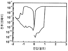
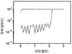
The primary technical challenges currently facing RRAM coating technology revolve around reliability, uniformity, and scalability. Device-to-device and cycle-to-cycle variability remains a significant obstacle, with switching parameters often showing inconsistency across multiple programming cycles. This variability stems largely from the stochastic nature of filament formation and rupture processes within the resistive switching layer, complicating efforts to achieve predictable performance in large arrays.
Endurance limitations represent another critical challenge, with many RRAM devices showing performance degradation after 10^6-10^9 switching cycles, falling short of the requirements for certain high-reliability applications. The degradation mechanisms include electrode material diffusion, oxygen vacancy migration, and structural changes in the switching layer during repeated cycling.
Retention characteristics at elevated temperatures present additional concerns, particularly for automotive and industrial applications where operating environments can be harsh. Current RRAM technologies often struggle to maintain data integrity beyond 10 years at temperatures exceeding 85°C, necessitating further material engineering and interface optimization.
From a manufacturing perspective, integration challenges with CMOS processes remain significant. The deposition of high-quality, uniform thin films at the nanoscale requires precise control over stoichiometry, crystallinity, and defect concentration. Atomic Layer Deposition (ALD) has emerged as a preferred technique for RRAM coating materials, though challenges in precursor chemistry and process optimization persist.
Geographically, research leadership in RRAM coating materials shows distinct patterns. East Asian countries, particularly South Korea, Japan, and Taiwan, dominate in terms of patent filings and commercial development, while European and North American institutions lead in fundamental materials science innovations. China has rapidly increased its research output in this field, particularly in novel material compositions and deposition techniques.
Recent breakthroughs in doped oxide systems and multilayer structures have shown promise in addressing some of these challenges, with improved retention and reduced variability. However, the path toward widespread commercial adoption requires further advances in material engineering, particularly in controlling defect chemistry and interface properties at the atomic scale.
State-of-the-Art RRAM Coating Material Solutions
01 Metal oxide materials for ReRAM
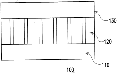
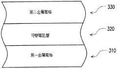
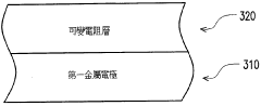
Metal oxides are widely used as resistive switching materials in ReRAM devices due to their excellent electrical properties and compatibility with semiconductor manufacturing processes. These materials include transition metal oxides such as hafnium oxide, titanium oxide, and tantalum oxide, which can form stable resistance states through oxygen vacancy migration. The coating methods for these materials often involve atomic layer deposition or sputtering techniques to achieve precise thickness control and uniformity across the device structure.- Metal oxide materials for RRAM devices: Metal oxide materials are widely used in resistive RAM devices due to their excellent switching characteristics. These materials include transition metal oxides such as hafnium oxide, titanium oxide, and tantalum oxide, which can be deposited as thin films using various coating techniques. The resistive switching behavior in these materials is attributed to the formation and rupture of conductive filaments, which can be controlled by applying appropriate voltage pulses.
- Deposition techniques for RRAM coating materials: Various deposition techniques are employed for coating materials in resistive RAM devices, including atomic layer deposition (ALD), chemical vapor deposition (CVD), physical vapor deposition (PVD), and sputtering. These techniques allow for precise control over film thickness, composition, and uniformity, which are critical factors affecting the performance and reliability of RRAM devices. The choice of deposition method depends on the specific material requirements and device architecture.
- Doped and composite materials for enhanced RRAM performance: Doping and forming composite materials can significantly enhance the performance of resistive RAM devices. By introducing dopants such as nitrogen, silicon, or rare earth elements into metal oxide films, or by creating multilayer structures with different materials, the switching characteristics, endurance, and retention properties of RRAM devices can be improved. These modified materials offer better control over the formation and rupture of conductive filaments, leading to more reliable and efficient memory operation.
- Polymer and organic materials for flexible RRAM: Polymer and organic materials are emerging as promising candidates for flexible and printable resistive RAM applications. These materials can be solution-processed and coated onto flexible substrates using techniques such as spin coating, inkjet printing, or spray coating. Conductive polymers, polymer composites with nanoparticles, and organic semiconductor materials offer advantages such as mechanical flexibility, low-temperature processing, and compatibility with roll-to-roll manufacturing for next-generation flexible electronics.
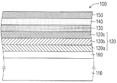
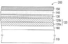
- Interface engineering and barrier layers in RRAM structures: Interface engineering and the incorporation of barrier layers play crucial roles in optimizing RRAM performance. By carefully designing the interfaces between different layers in the RRAM stack and introducing barrier layers, issues such as element diffusion, undesired reactions, and interface degradation can be mitigated. Materials such as titanium nitride, tantalum nitride, and silicon nitride are commonly used as barrier layers to improve device stability, uniformity, and endurance while preventing contamination during the fabrication process.
02 Chalcogenide-based resistive materials
Chalcogenide materials, particularly those containing elements such as germanium, antimony, and tellurium, are important for ReRAM applications due to their phase-change properties. These materials can switch between amorphous and crystalline states with different resistivity levels when subjected to electrical pulses. The coating processes for chalcogenide materials often require careful temperature control during deposition to ensure proper film composition and structure, which directly affects the switching performance and reliability of the ReRAM devices.Expand Specific Solutions03 Polymer and organic resistive materials
Polymer and organic materials offer unique advantages for flexible and printable ReRAM applications. These materials can be solution-processed at low temperatures, making them compatible with plastic substrates and roll-to-roll manufacturing. The resistive switching mechanism in these materials typically involves conformational changes or charge transfer processes. Various coating techniques such as spin coating, inkjet printing, and spray coating can be used to deposit these materials, enabling cost-effective fabrication of large-area memory devices with tunable electrical properties.Expand Specific Solutions04 Nanocomposite and doped coating materials
Nanocomposite materials combining conductive nanoparticles embedded in insulating matrices offer enhanced resistive switching performance for ReRAM applications. These materials benefit from the interfacial effects between the nanoparticles and the matrix, leading to more stable and controllable switching behavior. Additionally, doping conventional resistive materials with specific elements can modify their electrical properties and improve switching characteristics. Advanced coating techniques such as co-sputtering, sol-gel processing, and chemical vapor deposition are commonly used to achieve the desired nanostructure and composition.Expand Specific Solutions05 Multilayer and interface-engineered coatings
Multilayer structures consisting of different functional materials can significantly enhance the performance of ReRAM devices. By engineering the interfaces between these layers, the resistive switching behavior can be precisely controlled. These structures often include electrode materials, switching layers, and barrier layers to prevent undesired diffusion. The coating process for multilayer structures requires careful control of each layer's thickness and interface quality, often achieved through sequential deposition techniques such as atomic layer deposition or pulsed laser deposition, which allow for atomic-level precision in the fabrication process.Expand Specific Solutions
Leading Companies and Research Institutions in RRAM Field
The Resistive RAM coating materials market is currently in a growth phase, characterized by increasing investments and research activities. The market size is expanding due to rising demand for non-volatile memory solutions in IoT, AI, and data centers. Technologically, the field shows moderate maturity with established players like Samsung Electronics, SK Hynix, and Micron Technology leading commercial development, while specialized companies such as CrossBar and TetraMem focus on innovative RRAM implementations. Academic-industry collaborations involving Tsinghua University, KIST, and ITRI are accelerating material advancements. Taiwan Semiconductor, UMC, and SMIC represent the manufacturing infrastructure supporting this emerging technology, positioning RRAM coating materials as a critical component in next-generation memory solutions.
Samsung Electronics Co., Ltd.
Technical Solution: Samsung has pioneered advanced resistive RAM (ReRAM) coating materials through their innovative Metal-Oxide based solutions. Their technology utilizes hafnium oxide (HfOx) and tantalum oxide (TaOx) multi-layer structures that enable superior switching characteristics and retention properties. Samsung's ReRAM technology implements precise atomic layer deposition (ALD) techniques to create highly uniform and defect-controlled oxide films with thicknesses below 10nm[1]. Their proprietary oxygen vacancy control method allows for reliable resistance switching with endurance exceeding 10^6 cycles[3]. Samsung has also developed specialized doping strategies using metals like titanium and aluminum to engineer the conductive filament formation process, resulting in more stable and predictable memory performance. Recent advancements include their work on interface engineering between the electrode and switching layer to reduce variability and improve retention characteristics at smaller technology nodes[7].
Strengths: Industry-leading manufacturing capabilities with advanced 300mm fabrication facilities; extensive IP portfolio in ReRAM materials; strong vertical integration from materials research to product commercialization. Weaknesses: Higher production costs compared to conventional memory technologies; challenges in scaling below 20nm while maintaining performance consistency; relatively higher operating voltages compared to some competing technologies.
KIOXIA Corp.
Technical Solution: KIOXIA (formerly Toshiba Memory) has developed an innovative approach to ReRAM coating materials through their oxygen-engineered metal oxide technology. Their solution employs a sophisticated tantalum oxide-based switching layer with precisely controlled oxygen vacancy distribution to enable reliable resistive switching behavior. KIOXIA's proprietary deposition process combines reactive sputtering with carefully optimized thermal treatments to create a non-uniform oxygen concentration profile within the switching layer[3]. This engineered oxygen gradient facilitates the formation of conductive filaments along predetermined paths, resulting in more consistent switching characteristics and reduced cell-to-cell variability. Their technology incorporates specialized electrode materials with optimized work functions that lower the energy barrier for ion migration while maintaining excellent retention properties. KIOXIA has also pioneered the use of interface engineering techniques that create atomically sharp boundaries between the switching layer and electrodes, minimizing parasitic effects and improving overall device performance. Recent advancements include their development of multi-level cell capabilities that enable storage of 2 bits per cell, effectively doubling the memory density without increasing the physical footprint[10].
Strengths: Strong manufacturing capabilities with established high-volume production facilities; extensive experience in memory technologies; robust supply chain integration; advanced packaging technologies for system integration. Weaknesses: Higher forming voltages compared to some competing technologies; challenges in achieving uniform switching behavior at smaller technology nodes; relatively higher production costs due to complex material stack requirements.
Critical Patents and Research on Novel RRAM Coating Materials
Resistance random access memory and methods for manufacturing thereof
PatentInactiveTW200832677A
Innovation
- Employing platinum manganese compounds as the material for the metal electrodes, which are easier to etch and less expensive, facilitating improved process integration and reducing costs.
Resistive Random Access Memory
PatentActiveKR1020170016268A
Innovation
- A variable resistance memory structure comprising a substrate, a conductive layer, a copper-containing oxide layer, and an electron supply layer is introduced, where the electron supply layer suppresses copper filament diffusion and captures oxygen to enhance data retention and durability.
Manufacturing Scalability and Process Integration
The scalability of Resistive RAM (ReRAM) manufacturing processes represents a critical challenge in transitioning this promising memory technology from laboratory demonstrations to high-volume commercial production. Current coating material advancements must be evaluated not only for their electrical and physical properties but also for their compatibility with established semiconductor fabrication processes. The integration of novel ReRAM coating materials into existing CMOS manufacturing lines requires careful consideration of thermal budgets, contamination risks, and process compatibility.
Traditional physical vapor deposition (PVD) methods used for ReRAM coating materials face significant challenges when scaling to larger wafer sizes and higher throughput requirements. Recent developments in atomic layer deposition (ALD) techniques have shown promising results for achieving uniform, conformal coating of resistive switching materials with precise thickness control down to the atomic level. This advancement is particularly crucial as device dimensions continue to shrink below 20nm, where material uniformity directly impacts device-to-device variability.
Chemical vapor deposition (CVD) variants optimized specifically for transition metal oxides have demonstrated improved step coverage and composition control compared to conventional methods. These processes can be implemented on standard semiconductor manufacturing equipment with minimal modification, reducing capital expenditure barriers for mass production. Solution-based coating methods, including sol-gel processes and spin coating, offer cost-effective alternatives for certain material systems but face challenges in meeting the stringent uniformity requirements of high-density memory arrays.
Integration of ReRAM layers within the back-end-of-line (BEOL) process flow presents unique thermal constraints, as high-temperature annealing steps must be avoided to prevent damage to underlying interconnect structures. Recent innovations in low-temperature plasma-enhanced deposition techniques and rapid thermal processing have addressed this limitation, enabling the formation of high-quality resistive switching layers at temperatures below 400°C.
Yield management represents another critical aspect of manufacturing scalability. Advanced in-line metrology techniques, including spectroscopic ellipsometry and X-ray photoelectron spectroscopy, have been adapted for real-time monitoring of ReRAM coating material properties during production. These methods enable rapid process feedback and adjustment, essential for maintaining consistent device performance across large production volumes.
The economic viability of ReRAM technology depends heavily on achieving competitive cost structures through manufacturing optimization. Current cost models indicate that material selection plays a significant role in overall production economics, with simpler binary oxides offering advantages over more complex multi-component systems in terms of process complexity and yield. Industry leaders have begun establishing strategic partnerships with material suppliers to ensure consistent quality and supply chain reliability for specialized coating materials as production volumes increase.
Environmental Impact and Sustainability of RRAM Materials
The environmental impact of Resistive Random Access Memory (RRAM) materials has become increasingly important as electronic waste continues to accumulate globally. Traditional semiconductor manufacturing processes involve hazardous chemicals and significant energy consumption, making sustainability a critical consideration for next-generation memory technologies. RRAM offers potential advantages in this regard, particularly through innovations in coating materials that can reduce environmental footprint.
Current RRAM coating materials often include transition metal oxides such as HfO2, TiO2, and Ta2O5, which present varying degrees of environmental concerns. While these materials offer excellent switching properties, their extraction and processing can involve significant carbon emissions and resource depletion. Recent research has focused on developing more sustainable alternatives, including bio-derived materials and reduced-toxicity compounds that maintain performance while minimizing environmental impact.
Life cycle assessment (LCA) studies of RRAM materials reveal that the manufacturing phase contributes most significantly to their environmental footprint. Energy-intensive deposition techniques like atomic layer deposition (ALD) and sputtering account for substantial greenhouse gas emissions. Innovations in low-temperature deposition methods and energy-efficient coating processes are emerging as promising approaches to mitigate these impacts while maintaining device performance.
End-of-life considerations for RRAM devices present both challenges and opportunities. The complex multi-layer structure of RRAM cells complicates recycling efforts, but the relatively small quantities of precious metals compared to conventional memory technologies may reduce resource depletion. Research into design-for-disassembly approaches and selective recovery techniques for valuable materials is advancing, though commercial implementation remains limited.
Water usage represents another significant environmental concern in RRAM manufacturing. Conventional semiconductor processes require ultra-pure water in substantial quantities, contributing to water stress in manufacturing regions. Recent advancements in dry processing techniques and water recycling systems specifically designed for RRAM production show promise for reducing this impact, with some facilities reporting water usage reductions of up to 30%.
Regulatory frameworks are increasingly influencing RRAM material selection and manufacturing processes. The European Union's Restriction of Hazardous Substances (RoHS) directive and similar regulations worldwide are driving research toward inherently less toxic coating materials. This regulatory pressure, combined with corporate sustainability initiatives, is accelerating the development of environmentally benign alternatives to traditional RRAM materials, including lead-free compositions and reduced rare earth element content.
Unlock deeper insights with Patsnap Eureka Quick Research — get a full tech report to explore trends and direct your research. Try now!
Generate Your Research Report Instantly with AI Agent
Supercharge your innovation with Patsnap Eureka AI Agent Platform!