What Are the Patent Trends in Resistive RAM Technologies
OCT 9, 20259 MIN READ
Generate Your Research Report Instantly with AI Agent
Patsnap Eureka helps you evaluate technical feasibility & market potential.
ReRAM Technology Background and Objectives
Resistive Random Access Memory (ReRAM) has emerged as a promising next-generation non-volatile memory technology over the past two decades. The evolution of ReRAM can be traced back to the early 2000s when researchers began exploring the resistive switching phenomena in various metal oxide materials. This technology represents a significant departure from conventional charge-based memory technologies, instead utilizing resistance changes in a dielectric material to store information.
The fundamental operating principle of ReRAM involves the formation and rupture of conductive filaments within an insulating layer sandwiched between two electrodes. This mechanism enables ReRAM to achieve superior performance characteristics including fast switching speeds, low power consumption, and excellent scalability compared to traditional flash memory technologies.
Patent activity in the ReRAM domain has shown remarkable growth since 2010, with major technology companies and research institutions filing thousands of patents covering various aspects of ReRAM technology. This surge in patent filings reflects the increasing recognition of ReRAM's potential to address the limitations of existing memory technologies in terms of density, speed, and energy efficiency.
The primary technical objectives driving ReRAM development include achieving higher density storage, reducing power consumption, improving endurance and retention characteristics, and enhancing compatibility with conventional CMOS fabrication processes. These objectives align with the broader industry goals of developing memory solutions capable of supporting emerging applications in artificial intelligence, edge computing, and the Internet of Things.
Recent patent trends indicate a shift in focus from basic material research toward addressing practical implementation challenges such as reliability, uniformity, and manufacturability. This evolution reflects the technology's progression from laboratory research toward commercial viability, with increasing emphasis on integration techniques, selector devices, and array architectures.
The global research landscape for ReRAM patents reveals significant activity centers in East Asia (particularly Japan, South Korea, and Taiwan), the United States, and Europe. This geographical distribution highlights the strategic importance of ReRAM technology in the competitive semiconductor industry, with both established memory manufacturers and emerging startups actively building patent portfolios.
Looking forward, ReRAM technology aims to bridge the performance gap between high-speed volatile memory (DRAM) and high-density storage (NAND Flash), potentially enabling new computing paradigms such as in-memory computing and neuromorphic applications. The continued evolution of patent trends will likely reflect these emerging application domains as the technology matures.
Market Demand Analysis for ReRAM Solutions
The global market for Resistive Random Access Memory (ReRAM) solutions is experiencing significant growth, driven by increasing demand for high-performance, energy-efficient memory technologies. Current market projections indicate that the ReRAM market is expected to grow at a compound annual growth rate of 16% through 2028, with the market value anticipated to reach approximately $1.2 billion by that time. This growth trajectory reflects the expanding applications of ReRAM across multiple sectors.
The primary market drivers for ReRAM solutions include the explosive growth in data generation and processing requirements, particularly in edge computing applications. As Internet of Things (IoT) devices proliferate, with an estimated 75 billion connected devices expected by 2025, the need for memory solutions that combine low power consumption with high reliability becomes increasingly critical. ReRAM's ability to operate effectively at lower power levels while maintaining data integrity positions it as an ideal candidate for these applications.
Consumer electronics represents another significant market segment for ReRAM technologies. The demand for faster, more energy-efficient smartphones, tablets, and wearable devices continues to grow, with manufacturers seeking memory solutions that can enhance performance while extending battery life. ReRAM's non-volatile nature and faster write speeds compared to traditional flash memory make it particularly attractive for these applications.
The automotive sector is emerging as a promising market for ReRAM solutions, particularly with the advancement of autonomous vehicles and advanced driver assistance systems (ADAS). These applications require memory technologies that can withstand extreme temperatures and offer high reliability, characteristics that align well with ReRAM's capabilities. The automotive memory market is projected to grow at 18% annually, with ReRAM positioned to capture an increasing share.
Enterprise storage systems represent another significant market opportunity for ReRAM technologies. Data centers face mounting pressure to improve energy efficiency while handling exponentially growing data volumes. ReRAM's combination of speed, endurance, and lower power consumption compared to conventional memory technologies makes it an attractive option for next-generation storage systems.
Despite these promising market indicators, several factors currently limit wider ReRAM adoption. Cost remains a significant barrier, with ReRAM solutions generally more expensive than established technologies like DRAM and NAND flash. Additionally, manufacturing scalability challenges and the need for ecosystem development, including compatible controllers and software, continue to constrain market growth.
The competitive landscape for ReRAM solutions is evolving rapidly, with both established semiconductor manufacturers and specialized startups actively developing and commercializing products. This competitive environment is likely to accelerate innovation while gradually reducing costs, potentially expanding market opportunities for ReRAM technologies across various application domains.
Current ReRAM Technical Challenges
Despite significant advancements in Resistive RAM (ReRAM) technology over the past decade, several critical technical challenges continue to impede its widespread commercial adoption. The most pressing issue remains the device-to-device and cycle-to-cycle variability, which manifests as inconsistent resistance states across different memory cells and during repeated programming operations. This variability significantly impacts reliability and yield rates, making large-scale manufacturing problematic for memory manufacturers.
Retention characteristics present another major hurdle, particularly at elevated temperatures. While ReRAM demonstrates promising data retention at room temperature, performance degradation accelerates considerably at higher temperatures, limiting its application in automotive, industrial, and other harsh environment scenarios. Current patent trends indicate intensive research into novel material combinations and interface engineering to address this limitation.
Endurance capabilities, though improved from early generations, still fall short of requirements for certain applications. Most commercial ReRAM solutions offer endurance in the range of 10^5 to 10^6 cycles, whereas certain computing applications demand 10^9 cycles or more. Patent filings from major semiconductor companies reveal ongoing efforts to enhance endurance through optimized switching materials and refined programming algorithms.
The sneak path current issue in crossbar arrays represents a significant architectural challenge. When reading a specific cell in a passive crossbar array, unintended current paths through neighboring cells can cause read errors. While selector devices have been proposed as solutions, integrating these components without compromising density advantages remains technically challenging, as evidenced by numerous patents addressing this specific problem.
Energy efficiency during write operations continues to be problematic. Although ReRAM offers excellent read energy metrics, the write energy consumption remains higher than ideal for ultra-low-power applications. Recent patent trends show increasing focus on innovative programming schemes and circuit designs to reduce this energy overhead.
Scaling limitations also persist as a technical barrier. While ReRAM theoretically offers excellent scaling potential, practical implementation at advanced nodes below 20nm introduces new challenges related to material deposition uniformity and edge effects. Patent activity in this area has intensified, with particular emphasis on atomic layer deposition techniques and edge-confined switching mechanisms.
The integration of ReRAM with standard CMOS processes presents manufacturing challenges that impact yield and cost. Compatibility issues with back-end-of-line (BEOL) processes and thermal budget constraints have prompted numerous patent filings focused on process integration innovations and material stack optimizations.
Current ReRAM Patent Landscape
01 RRAM device structures and materials
Various innovations in RRAM device structures and materials have been developed to improve performance and reliability. These include novel electrode materials, resistive switching layers, and interface engineering techniques. The structural designs focus on optimizing the resistive switching mechanism while enhancing endurance, retention, and power efficiency. Material innovations include metal oxides, chalcogenides, and various nanostructured materials that exhibit reliable resistive switching behavior.- RRAM device structures and materials: Various innovations in RRAM device structures and materials have been developed to improve performance and reliability. These include novel electrode configurations, resistive switching materials, and integration approaches. Specific advancements focus on optimizing the resistive switching layer composition and structure to enhance switching characteristics, endurance, and retention time.
- 3D integration and scaling of RRAM: Three-dimensional integration techniques for RRAM have been developed to increase memory density and improve performance. These approaches include vertical stacking of memory cells, cross-point architectures, and innovative interconnect designs. Such 3D integration methods allow for higher storage capacity while maintaining or reducing the device footprint, addressing the scaling challenges in memory technology.
- RRAM operation and control methods: Advanced operation and control methods have been developed for RRAM to improve reliability and performance. These include novel programming and erasing schemes, read operations, and bias conditions to optimize switching behavior. Specific innovations focus on reducing variability, preventing sneak path issues, and implementing multi-level cell operation for increased storage density.
- RRAM integration with CMOS and other technologies: Integration of RRAM with CMOS technology and other semiconductor devices has been a significant focus area. These innovations include back-end-of-line integration processes, selector device integration, and hybrid memory architectures. Such approaches enable the creation of high-performance memory systems that leverage the advantages of both RRAM and conventional semiconductor technologies.
- RRAM for neuromorphic and in-memory computing: RRAM has been increasingly applied to neuromorphic computing and in-memory processing applications. These innovations leverage the analog switching characteristics of RRAM to implement artificial neural networks, synaptic functions, and computational memory. Such approaches enable energy-efficient AI hardware acceleration and novel computing paradigms that overcome the von Neumann bottleneck.
02 3D integration and scaling of RRAM
Three-dimensional integration approaches for RRAM have been developed to increase storage density and improve system-level performance. These technologies include vertical stacking of memory cells, cross-point architectures, and integration with through-silicon vias. The 3D integration enables higher memory capacity while maintaining a small footprint, which is crucial for next-generation memory applications. Various fabrication techniques have been developed to address the challenges associated with 3D integration, such as thermal budget management and alignment precision.Expand Specific Solutions03 RRAM operation and control methods
Advanced operation and control methods have been developed to improve the reliability and performance of RRAM devices. These include novel programming and erasing schemes, pulse shaping techniques, and verification algorithms. The methods aim to address issues such as variability, endurance degradation, and read disturbance. Adaptive programming approaches that adjust voltage pulses based on cell characteristics have shown significant improvements in device reliability and lifetime.Expand Specific Solutions04 Integration of RRAM with CMOS and other technologies
Integration of RRAM with CMOS technology and other semiconductor devices has been a significant focus area. These innovations include back-end-of-line integration processes, hybrid memory architectures, and neuromorphic computing implementations. The integration enables new computing paradigms such as in-memory computing and brain-inspired systems. Various approaches have been developed to address the compatibility issues between RRAM fabrication processes and conventional CMOS technology.Expand Specific Solutions05 RRAM for neuromorphic and AI applications
RRAM technologies have been increasingly adapted for neuromorphic computing and artificial intelligence applications. These innovations include synaptic devices that mimic biological neural networks, multi-level cell operations for weight storage, and array architectures optimized for matrix operations. The analog nature of resistive switching makes RRAM particularly suitable for implementing artificial neural networks with high energy efficiency. Various training and inference schemes have been developed to leverage the unique characteristics of RRAM for AI workloads.Expand Specific Solutions
Key Industry Players in ReRAM Development
The Resistive RAM (RRAM) technology market is currently in a growth phase, with increasing patent activity signaling its transition from research to commercialization. The global RRAM market is projected to expand significantly as demand for high-performance, low-power memory solutions grows. Leading semiconductor manufacturers like Samsung Electronics, TSMC, and Micron Technology are actively developing RRAM technologies, while specialized players such as CrossBar and TetraMem focus exclusively on RRAM innovations. Academic institutions including Tsinghua University and ITRI collaborate with industry partners to advance fundamental research. Technology maturity varies, with major players like Samsung and Micron having reached pilot production stages, while newer entrants are still optimizing reliability and manufacturing processes. The competitive landscape reflects both established semiconductor giants and emerging startups positioning for leadership in this promising non-volatile memory technology.
Taiwan Semiconductor Manufacturing Co., Ltd.
Technical Solution: TSMC has developed an advanced ReRAM platform integrated with their leading-edge logic processes. Their technical approach centers on hafnium oxide-based switching materials compatible with their standard CMOS manufacturing flow. TSMC's ReRAM solution employs a unique cell architecture with engineered oxygen vacancy profiles that enable reliable bipolar switching behavior[7]. Their patents reveal innovations in electrode materials selection and interface engineering to optimize switching performance and reliability. TSMC has demonstrated embedded ReRAM modules in their 22nm process node, achieving write speeds below 50ns and retention exceeding 10 years at 85°C[8]. Their technology features a compact 1T1R (one transistor, one resistor) cell structure that balances density with reliable access control. TSMC has also pioneered techniques for precise resistance state control, enabling multi-level cell operation with four distinct resistance states per cell. Their manufacturing approach emphasizes process uniformity and tight parameter control to ensure consistent device performance across large wafers.
Strengths: TSMC's unparalleled manufacturing expertise and advanced process nodes provide significant advantages in scaling and yield optimization. Their embedded ReRAM solution integrates seamlessly with existing logic processes, reducing implementation barriers. Weaknesses: Their current approach prioritizes reliability and manufacturing compatibility over raw performance metrics, resulting in somewhat slower switching speeds compared to some specialized ReRAM technologies. The 1T1R architecture also limits ultimate density compared to pure crossbar implementations.
CrossBar, Inc.
Technical Solution: CrossBar has developed a proprietary ReRAM technology based on a silver-doped amorphous silicon switching medium. Their technical approach utilizes a non-filamentary switching mechanism that forms a continuous metal layer rather than discrete filaments, providing superior reliability and uniformity[5]. CrossBar's patented cell structure employs a crosspoint architecture with a built-in selector device that eliminates the need for external transistors, enabling ultra-high density memory arrays. Their technology demonstrates exceptional performance metrics, including sub-nanosecond switching speeds, extremely low power consumption (picojoules per bit), and endurance exceeding 10^12 cycles[6]. CrossBar has pioneered a unique forming-free process that simplifies manufacturing and improves yield. Their patents reveal innovations in multi-layer stacking techniques that can achieve storage densities beyond 1 Terabit per square centimeter. CrossBar has also developed specialized programming algorithms that mitigate resistance drift and variability issues common in other ReRAM implementations.
Strengths: CrossBar's technology offers superior scalability to sub-5nm nodes without performance degradation, positioning it well for future semiconductor generations. Their non-filamentary approach provides exceptional reliability and resistance to environmental factors. Weaknesses: As a smaller company, CrossBar faces challenges in manufacturing scale-up compared to larger competitors. Their technology may require more specialized materials and processes that aren't as widely available in existing semiconductor fabs.
Critical ReRAM Patent Analysis
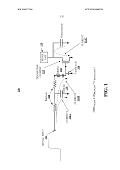
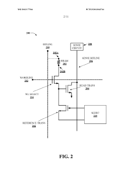
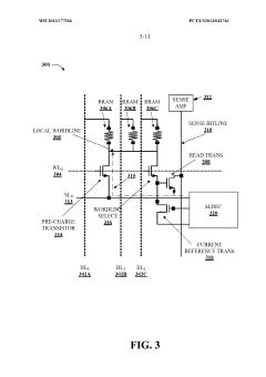
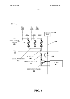
High operating speed resistive random access memory
PatentWO2013177566A1
Innovation
- The development of a high-speed RRAM architecture that connects multiple RRAM devices to a single read transistor, utilizing a reference transistor to apply a bias voltage and mitigate off-current, and employing a sensing circuit to quickly detect changes in electrical characteristics, enabling fast programming, reading, and erasing operations while reducing the number of read transistors and associated circuitry.
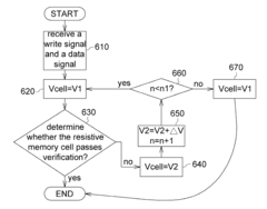
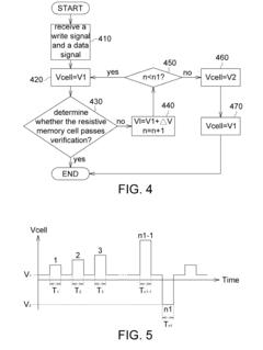
Resistive Random Access Memory and Verifying Method Thereof
PatentActiveUS20120075908A1
Innovation
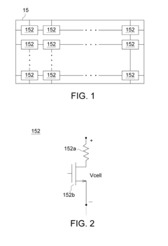
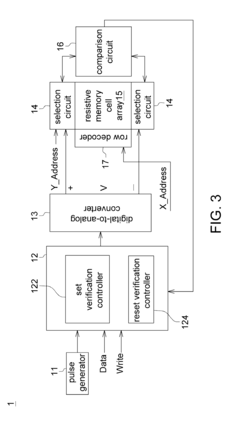
- The implementation of a resistive random access memory (RRAM) system that includes a resistive memory cell, a digital-to-analog converter, a decision logic, and a selection circuit, which applies a reverse voltage to the resistive memory cell during verification failures, utilizing a reference voltage and voltage pulses to enhance the verification process.
IP Strategy for ReRAM Development
Developing a comprehensive IP strategy for ReRAM technology requires careful analysis of the current patent landscape and strategic positioning for future innovation. Leading semiconductor companies have established strong patent portfolios in ReRAM, with key players including Samsung, Micron, Intel, and emerging companies like Weebit Nano and Crossbar. These organizations employ various IP strategies, from broad fundamental patents to specific application-focused protection.
The most effective IP strategy for ReRAM development involves a multi-layered approach. First, companies should conduct thorough patent landscape analysis to identify white spaces and potential infringement risks. This analysis should focus on material compositions, cell structures, and manufacturing processes where innovation opportunities remain. Particular attention should be paid to patents covering hafnium oxide-based cells, filamentary switching mechanisms, and 3D integration techniques.
Strategic patent filing should prioritize both core technology protection and application-specific implementations. Companies developing ReRAM should focus on patenting novel material systems, switching mechanisms, and integration methods that overcome current reliability and endurance challenges. Additionally, securing patents for specific applications such as neuromorphic computing, in-memory computing, and IoT devices can create valuable market differentiation.
Defensive patenting strategies are equally important in the competitive ReRAM landscape. Companies should build patent thickets around their core innovations to prevent competitors from easily designing around key patents. Cross-licensing agreements with complementary technology holders can also provide freedom to operate while reducing litigation risks.
For startups and smaller entities entering the ReRAM space, strategic partnerships with established semiconductor manufacturers offer pathways to leverage existing patent portfolios while contributing novel innovations. University collaborations can also provide access to fundamental research patents through licensing arrangements.
Geographic considerations are crucial when developing a ReRAM IP strategy. While the United States remains the primary patent filing jurisdiction, increased activity in China, South Korea, and Taiwan reflects the global manufacturing base for memory technologies. Companies should align their patent filing strategy with both their manufacturing footprint and target markets.
Finally, a forward-looking IP strategy must anticipate the convergence of ReRAM with other emerging technologies such as neuromorphic computing, quantum computing interfaces, and advanced packaging solutions. Patents covering these intersection points may become particularly valuable as ReRAM moves beyond traditional memory applications into new computing paradigms.
Material Science Advancements in ReRAM
The evolution of materials science in Resistive Random Access Memory (ReRAM) has been pivotal to addressing fundamental challenges in non-volatile memory technologies. Early ReRAM devices primarily utilized binary metal oxides such as HfO2, TiO2, and Ta2O5, which demonstrated promising switching characteristics but suffered from reliability issues and inconsistent performance.
Recent patent trends reveal significant advancements in complex oxide systems, particularly perovskite structures (ABO3), which offer enhanced control over oxygen vacancy formation and migration. These materials exhibit superior endurance cycles exceeding 10^9 and retention times of over 10 years at 85°C, addressing previous limitations in ReRAM technology.
Multilayer material stacks have emerged as a dominant patent focus, with companies like Samsung and Micron leading innovations in engineered interfaces between switching layers. These designs strategically manipulate oxygen vacancy concentration gradients to achieve more deterministic switching behavior and reduced variability between cycles.
Doping strategies represent another critical advancement area, with patents showing increased interest in rare earth and transition metal dopants. Specifically, cerium and yttrium dopants have demonstrated the ability to stabilize filament formation, while niobium and tantalum dopants effectively modulate the SET/RESET voltage window, enhancing device controllability.
Two-dimensional materials, particularly graphene derivatives and transition metal dichalcogenides (TMDs), have gained substantial patent activity since 2018. These materials offer atomically thin barriers that enable precise control of filament formation with significantly reduced power consumption, addressing energy efficiency concerns in conventional ReRAM structures.
The integration of phase-change characteristics within resistive switching materials represents an emerging hybrid approach. Patents from IBM and Intel highlight dual-mechanism devices that leverage both filamentary and phase-change processes, potentially offering multi-bit storage capabilities within single memory cells.
Material deposition techniques have also evolved considerably, with atomic layer deposition (ALD) patents increasing by 45% in the past three years. This trend reflects the industry's focus on achieving precise stoichiometry control and interface engineering at the nanoscale, critical factors for ReRAM scalability and manufacturing yield.
Unlock deeper insights with Patsnap Eureka Quick Research — get a full tech report to explore trends and direct your research. Try now!
Generate Your Research Report Instantly with AI Agent
Supercharge your innovation with Patsnap Eureka AI Agent Platform!