

Exploring Resistive RAM in Next-Gen Electronics
OCT 9, 20259 MIN READ
Generate Your Research Report Instantly with AI Agent
PatSnap Eureka helps you evaluate technical feasibility & market potential.
ReRAM Technology Background and Objectives
Resistive Random Access Memory (ReRAM) represents a revolutionary advancement in non-volatile memory technology, emerging as a promising alternative to conventional memory solutions. The evolution of ReRAM can be traced back to the early 2000s when researchers began exploring the resistive switching phenomena in various metal oxide materials. This technology leverages the ability of certain materials to change their resistance state when subjected to electrical stimuli, enabling data storage through resistance variations rather than electron charge.
The development trajectory of ReRAM has been characterized by significant milestones, including the demonstration of reliable switching behavior in metal oxides like HfO2 and TiO2, the achievement of multi-level cell capabilities, and the integration with CMOS technology. Recent advancements have focused on enhancing endurance, reducing power consumption, and improving switching speed, positioning ReRAM as a viable contender in the memory hierarchy.
The primary technical objective in ReRAM research is to overcome the limitations of traditional memory technologies, particularly in terms of scalability, energy efficiency, and performance. As conventional memory approaches their physical scaling limits, ReRAM offers a pathway to continue Moore's Law-like progression in memory density and performance. Specifically, researchers aim to develop ReRAM solutions that combine the speed of SRAM, the density of DRAM, and the non-volatility of flash memory.
Current technical goals include achieving sub-nanosecond switching speeds, endurance exceeding 10^12 cycles, retention times of over 10 years, and ultra-low power operation. Additionally, there is a strong focus on addressing variability issues, enhancing reliability, and developing robust manufacturing processes suitable for high-volume production.
The technology trend indicates a shift towards three-dimensional architectures, integration with neuromorphic computing systems, and exploration of novel materials beyond metal oxides. The convergence of ReRAM with emerging computing paradigms, such as in-memory computing and brain-inspired architectures, represents a significant direction in its evolution.
From an industry perspective, ReRAM is positioned to address critical challenges in next-generation electronics, including the memory wall problem, energy constraints in mobile and IoT devices, and the increasing demands of artificial intelligence applications. The technology's potential to enable new computing architectures and enhance system performance makes it a strategic focus for both academic research and industrial development.
As we look towards future applications, ReRAM is expected to play a pivotal role in edge computing, autonomous systems, and advanced AI implementations, where its unique combination of speed, energy efficiency, and non-volatility offers compelling advantages over existing solutions.
Market Demand Analysis for Non-Volatile Memory
The non-volatile memory market is experiencing unprecedented growth driven by the proliferation of data-intensive applications across multiple sectors. Current market valuations place the global non-volatile memory market at approximately 62 billion USD in 2023, with projections indicating a compound annual growth rate (CAGR) of 12.3% through 2030. This robust expansion reflects the increasing demand for high-performance, energy-efficient memory solutions that can support emerging technologies.
Resistive RAM (ReRAM) represents a particularly promising segment within this market, addressing critical limitations of conventional memory technologies. Industry analysts have identified several key demand drivers propelling interest in ReRAM and similar next-generation non-volatile memory technologies.
The explosion of Internet of Things (IoT) devices presents perhaps the most significant market opportunity. With connected device installations expected to reach 75 billion by 2025, the demand for low-power, high-endurance memory solutions is accelerating rapidly. ReRAM's ability to operate with minimal power consumption while maintaining data integrity makes it ideally suited for edge computing applications where energy efficiency is paramount.
Data centers and cloud infrastructure providers constitute another major market segment driving demand. As organizations process increasingly massive datasets, memory performance has become a critical bottleneck in system architecture. ReRAM's potential to deliver DRAM-like speeds with non-volatile storage capabilities addresses this challenge directly, with early benchmarks showing up to 10x improvement in energy efficiency compared to conventional solutions.
The automotive sector represents a rapidly expanding market for advanced non-volatile memory, particularly with the rise of autonomous vehicles. These systems require memory technologies that can withstand extreme operating conditions while delivering ultra-fast read/write capabilities for real-time decision making. Market research indicates that automotive memory requirements are growing at 25% annually, outpacing most other sectors.
Consumer electronics manufacturers are also driving demand, seeking memory solutions that can enable thinner devices with longer battery life. The smartphone market alone, with annual shipments exceeding 1.3 billion units, represents a massive potential market for ReRAM technology.
Enterprise storage systems are increasingly adopting tiered memory architectures, creating opportunities for ReRAM to serve as a bridge between high-speed DRAM and high-capacity storage. This "storage class memory" segment is projected to grow substantially as organizations seek to optimize their data processing capabilities.
Despite these promising indicators, market adoption faces challenges including manufacturing scalability, cost competitiveness with established technologies, and integration complexities. However, the clear trajectory of increasing demand across multiple sectors suggests ReRAM and similar next-generation non-volatile memory technologies are positioned for significant market penetration in the coming decade.
ReRAM Development Status and Technical Challenges
Resistive RAM (ReRAM) technology has emerged as a promising candidate for next-generation non-volatile memory solutions, offering advantages in power efficiency, scalability, and integration potential. Currently, ReRAM development has reached a critical juncture where laboratory demonstrations have proven its fundamental viability, yet significant challenges remain before widespread commercial adoption can occur.
The global ReRAM landscape shows varied development progress across regions. North America leads in fundamental research with institutions like Stanford University and companies such as Crossbar and Weebit Nano making significant advancements. Asia, particularly Japan, South Korea, and Taiwan, dominates in manufacturing infrastructure development, with companies like Fujitsu, Samsung, and TSMC investing heavily in ReRAM production capabilities. European research centers focus on materials science innovations to overcome reliability barriers.
Current technical challenges primarily revolve around four key areas. First, endurance limitations restrict ReRAM to approximately 10^6 to 10^7 write cycles, significantly below the 10^12 cycles achieved by SRAM. This limitation stems from physical degradation of the switching material during repeated programming operations, causing eventual device failure.
Second, retention stability presents a critical obstacle, with data retention periods varying from months to years depending on operating conditions. Environmental factors such as temperature fluctuations can accelerate data degradation, complicating deployment in automotive and industrial applications where extreme conditions are common.
Third, variability in switching behavior between cells and even within the same cell over time creates reliability concerns. This cell-to-cell and cycle-to-cycle variability necessitates complex error correction mechanisms that increase system overhead and power consumption.
Fourth, scaling challenges emerge as ReRAM cells approach sub-10nm dimensions. At these scales, quantum effects and material interface phenomena become increasingly dominant, potentially altering the fundamental switching mechanisms that enable ReRAM operation.
Manufacturing integration represents another significant hurdle. While ReRAM offers theoretical CMOS compatibility, practical implementation requires specialized materials and processes that may not align with standard semiconductor fabrication flows. The introduction of new materials like hafnium oxide, tantalum oxide, or complex metal oxides demands careful consideration of contamination risks and process compatibility.
Power consumption during write operations, though improved compared to flash memory, remains higher than ideal for ultra-low-power applications. The fundamental physics of filament formation and rupture requires voltage thresholds that establish minimum energy requirements for reliable operation.
Despite these challenges, recent breakthroughs in materials engineering and device architecture suggest pathways toward solutions. Multi-layer oxide structures have demonstrated improved endurance characteristics, while doped switching materials show promise for enhancing retention stability without sacrificing switching speed.
Current ReRAM Implementation Approaches
01 Resistive RAM device structures
Resistive RAM (RRAM) devices are constructed with specific structural configurations to optimize performance. These structures typically include a resistive switching layer sandwiched between two electrodes. Various materials can be used for the resistive layer, including metal oxides, chalcogenides, and perovskites. The electrode materials and interface engineering play crucial roles in determining switching characteristics. Advanced structures may incorporate additional layers for improved stability, retention, and endurance.- Resistive RAM device structures: Resistive RAM (RRAM) devices are typically constructed with specific structural configurations to optimize performance. These structures often include a resistive switching layer sandwiched between two electrodes. Various materials can be used for the resistive layer, including metal oxides, chalcogenides, and perovskites. The electrode materials and their interfaces with the resistive layer play crucial roles in determining switching characteristics. Advanced RRAM structures may incorporate additional layers for improved stability, retention, and endurance.
- Resistive switching mechanisms: The operation of resistive RAM relies on various switching mechanisms that change the resistance state of the memory cell. These mechanisms include filamentary conduction, where conductive filaments form and rupture within the resistive layer; interface-type switching, where the resistance changes at the electrode-oxide interface; and phase change, where the material undergoes structural transformation. Understanding these mechanisms is essential for designing reliable RRAM devices with consistent switching behavior, low power consumption, and high endurance.
- Materials for resistive RAM: Material selection is critical for resistive RAM performance. Common materials include transition metal oxides (such as HfOx, TaOx, TiOx), chalcogenides (like GeSbTe), and complex oxides (such as perovskites). The choice of electrode materials also significantly impacts device characteristics, with noble metals, conducting nitrides, and doped semiconductors being commonly used. Novel material systems and combinations are continuously being explored to enhance switching speed, reduce operating voltage, improve retention time, and increase the number of reliable switching cycles.
- Integration and fabrication techniques: Fabrication and integration of resistive RAM into existing semiconductor processes present significant challenges. Various techniques are employed, including atomic layer deposition, physical vapor deposition, and solution-based methods for resistive layer formation. 3D integration approaches, such as crossbar arrays and vertical stacking, enable high-density memory architectures. Process optimization is crucial to ensure uniformity, reduce variability, and maintain compatibility with CMOS technology. Advanced patterning and etching techniques are developed to achieve smaller feature sizes and higher integration densities.
- Circuit design and operation schemes: Circuit design plays a vital role in resistive RAM implementation. Specialized sensing circuits are required to detect the resistance states accurately. Programming schemes must control current compliance to prevent device damage during set/reset operations. Various architectures have been developed, including 1T1R (one transistor, one resistor), crossbar arrays, and complementary resistive switching configurations. Advanced operation schemes address issues like sneak path currents in crossbar arrays and implement multi-level cell operation for increased storage density. Peripheral circuits for addressing, programming, and reading operations are optimized for power efficiency and reliability.
02 Resistive switching mechanisms
The operation of RRAM relies on resistive switching mechanisms that allow the device to toggle between high and low resistance states. These mechanisms include filamentary conduction, where conductive filaments form and rupture within the switching layer, and interface-type switching, where the resistance change occurs at the electrode-oxide interface. The switching can be categorized as unipolar or bipolar depending on the voltage polarity requirements. Understanding these mechanisms is essential for designing reliable RRAM devices with consistent performance characteristics.Expand Specific Solutions03 Materials for RRAM fabrication
Material selection is critical for RRAM performance. Common resistive switching materials include transition metal oxides (HfOx, TaOx, TiOx), chalcogenides (GeSe, GeS), and complex oxides. Electrode materials range from noble metals (Pt, Au) to reactive metals (Ti, Ta) and conducting nitrides (TiN, TaN). Doping the switching layer with specific elements can enhance switching characteristics and reliability. Novel 2D materials and nanocomposites are being explored to improve performance metrics such as switching speed, power consumption, and retention time.Expand Specific Solutions04 RRAM array architecture and integration
RRAM can be integrated into various memory array architectures, including crossbar arrays, 3D stacked structures, and hybrid systems. These architectures address challenges like sneak path currents and enable high-density storage. Integration with CMOS technology is essential for practical applications, requiring compatible fabrication processes and addressing interface issues. Selector devices are often incorporated to prevent interference between memory cells. Advanced architectures may include multi-level cell capabilities to increase storage density.Expand Specific Solutions05 RRAM applications and performance optimization
RRAM finds applications in non-volatile memory, neuromorphic computing, and in-memory computing systems. Performance optimization involves techniques such as pulse engineering to control the set and reset operations, temperature management to ensure stability, and error correction schemes to improve reliability. Circuit design considerations include sense amplifiers for accurate readout and programming circuits for precise resistance control. Emerging applications include security primitives like physical unclonable functions and true random number generators based on the inherent stochasticity of resistive switching.Expand Specific Solutions
Key Industry Players in ReRAM Development
Resistive RAM (ReRAM) technology is currently in the early growth phase of its development cycle, with the global market expected to reach significant expansion as next-generation electronics demand more efficient memory solutions. The competitive landscape features established semiconductor giants like Samsung Electronics, SK Hynix, and Micron Technology investing heavily in ReRAM research, alongside specialized players such as CrossBar and Adesto Technologies who are pioneering innovative implementations. Asian manufacturers, particularly TSMC, KIOXIA, and Chinese entities like SMIC, are rapidly advancing their capabilities to challenge traditional market leaders. The technology is approaching commercial maturity for specific applications, with companies demonstrating working prototypes and early production units, though widespread adoption faces challenges in scaling, endurance, and manufacturing consistency.
Samsung Electronics Co., Ltd.
Technical Solution: 三星电子开发了一种基于金属氧化物的ReRAM技术,采用HfO2(氧化铪)作为核心开关材料。其技术方案采用垂直堆叠架构(V-ReRAM),通过在单个芯片上垂直堆叠多层ReRAM单元,大幅提高存储密度。三星的ReRAM单元由顶部电极、HfO2开关层、TiN(氮化钛)扩散层和底部电极组成。当施加电压时,氧空位在HfO2中形成导电通路,实现电阻状态切换。为解决ReRAM的可靠性问题,三星开发了专利的"自限制电流"技术,通过在单元中集成电流限制层,防止形成过大的导电细丝,显著提高了器件稳定性和耐久性。此外,三星还实现了ReRAM与其先进的3D制造工艺的结合,开发出"3D-ReRAM"架构,每个垂直通道可容纳多达128层存储单元。三星还针对ReRAM特性优化了存储控制器,开发了专用的磨损均衡算法和错误校正码,进一步提高了系统可靠性。
优势:三星的ReRAM技术具有极高的集成度和存储密度,读写速度比NAND闪存快100倍,功耗低,且与其现有的3D制造工艺兼容,便于大规模生产。三星强大的供应链和制造能力也是其显著优势。劣势:其垂直堆叠架构增加了制造复杂性和成本;在高温环境下,多层堆叠结构的热稳定性仍需改进;技术成熟度相对较低,尚未实现大规模商业化。
Micron Technology, Inc.
Technical Solution: 美光科技开发了一种基于氧化物的ReRAM技术,采用专有的双层金属氧化物结构。其技术方案中,每个存储单元由两层不同的金属氧化物组成:一层作为开关层,另一层作为氧储存层。这种双层设计能更精确地控制氧离子迁移,提高了器件的稳定性和可靠性。美光的ReRAM采用1T1R(一个晶体管一个电阻)结构,每个存储单元与一个访问晶体管配对,有效解决了大规模阵列中的串扰问题。为提高存储密度,美光开发了多位存储技术,通过精确控制导电细丝的形成过程,在单个单元中实现4-8个不同电阻状态,相当于存储2-3位数据。美光还针对ReRAM特性开发了专用的编程算法,采用自适应脉冲调制技术,根据单元特性动态调整编程电压和时间,显著提高了写入速度和可靠性。此外,美光还实现了ReRAM与其3D XPoint技术的结合,开发出混合架构存储解决方案,兼具高性能和高密度特性。
优势:美光的ReRAM技术具有出色的耐久性(超过10^9次写入/擦除循环)、快速的切换速度(10ns级)和低功耗特性。其1T1R结构提供了优异的读写性能和可靠性,且与现有CMOS工艺高度兼容。美光在存储器领域的丰富经验也是其显著优势。劣势:1T1R结构限制了存储密度的提升;多位存储模式下的可靠性和耐久性有所降低;制造成本相对较高,尤其是在大容量应用场景中。
Critical Patents and Technical Innovations in ReRAM
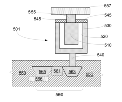
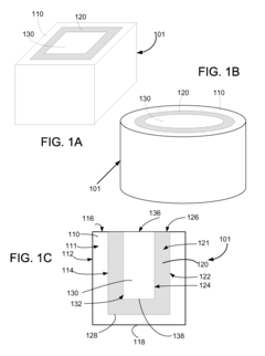
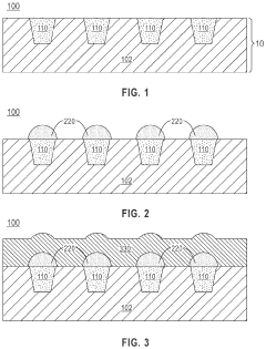
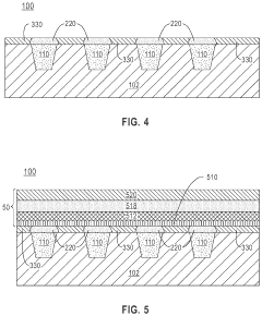
Structures for resistive random access memory cells
PatentActiveUS7791925B2
Innovation
- The RRAM cell design features a trench structure with a first electrode, a resistive layer, and a second electrode, where the resistive layer is nested inside the first electrode, and the second electrode is nested inside the resistive layer, increasing the contact area between the electrodes and the resistive layer, thereby enhancing the cell's functionality.
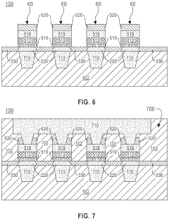
High-density resistive random-access memory array with self-aligned bottom electrode contact
PatentActiveUS11856878B2
Innovation
- A self-aligned bottom electrode is formed using selective deposition methods, eliminating the need for patterning and reducing misalignment, with a semi-circular shape to simplify the manufacturing process and enhance scalability.
Material Science Advancements for ReRAM
The evolution of Resistive Random Access Memory (ReRAM) technology has been significantly influenced by breakthroughs in material science. Traditional ReRAM structures relied primarily on binary metal oxides such as HfO2, TiO2, and Ta2O5, which offered reasonable performance but faced challenges in switching uniformity and retention. Recent advancements have shifted focus toward complex oxide systems and novel material combinations that dramatically enhance device characteristics.
Perovskite-structured materials have emerged as promising candidates for next-generation ReRAM devices. These materials, with their general formula ABO3, demonstrate exceptional ionic conductivity and tunable resistance states. Research indicates that strontium titanate (SrTiO3) and lanthanum nickelate (LaNiO3) based structures exhibit superior switching ratios exceeding 103 while maintaining switching endurance beyond 106 cycles.
Two-dimensional (2D) materials represent another frontier in ReRAM development. Graphene oxide, MoS2, and hexagonal boron nitride (h-BN) have demonstrated remarkable capabilities as switching layers. The atomically thin nature of these materials enables precise control over filament formation and dissolution processes. Studies show that graphene oxide-based ReRAM can achieve sub-5 ns switching speeds with energy consumption below 0.1 pJ per switching event.
Interface engineering has become a critical aspect of ReRAM material science. The controlled formation of oxygen vacancies at material interfaces significantly influences switching behavior. Recent research demonstrates that inserting thin buffer layers (1-3 nm) of materials like Al2O3 between the active layer and electrodes can enhance retention time by over 200% while reducing cycle-to-cycle variability.
Electrode material selection has proven equally important in ReRAM development. Moving beyond traditional noble metals, researchers have explored reactive electrodes such as Ti, Ta, and Hf that actively participate in the switching mechanism. These materials form localized regions of oxygen deficiency, creating preferential paths for filament formation and resulting in more predictable switching behavior.
Doping strategies have revolutionized ReRAM material performance. Introducing controlled concentrations of elements such as Cu, Ag, or rare earth metals into the switching layer modifies the electronic structure and defect chemistry. For instance, Gd-doped HfO2 demonstrates a 40% reduction in forming voltage while maintaining a high ON/OFF ratio, addressing one of the key challenges in ReRAM commercialization.
Energy Efficiency and Sustainability Aspects
Resistive RAM (ReRAM) technology represents a significant advancement in energy-efficient computing architectures. When examining the energy efficiency profile of ReRAM, we observe substantial advantages over conventional memory technologies. ReRAM cells typically consume 10-100 times less power during operation compared to flash memory, with switching energies as low as 0.1-1 pJ per bit. This remarkable efficiency stems from ReRAM's fundamental operating principle, which requires minimal current to change resistance states.
The standby power consumption of ReRAM arrays further enhances their sustainability credentials. Unlike DRAM which requires constant refresh operations consuming background power, ReRAM maintains stored information without continuous power input, resulting in near-zero standby power consumption. This characteristic makes ReRAM particularly valuable for edge computing devices and IoT applications where battery life and energy conservation are critical constraints.
From a manufacturing perspective, ReRAM offers compelling sustainability advantages. The fabrication process typically requires fewer mask layers and processing steps compared to conventional memory technologies, translating to reduced material consumption and manufacturing energy requirements. Additionally, many ReRAM structures utilize abundant materials like silicon oxide, titanium oxide, or hafnium oxide, potentially reducing reliance on rare or environmentally problematic elements found in some conventional memory technologies.
Thermal efficiency represents another significant sustainability aspect of ReRAM technology. The reduced operating currents result in lower heat generation during operation, which cascades into system-level benefits including reduced cooling requirements and extended device lifespans. This thermal efficiency becomes increasingly important as computing devices continue to shrink while processing demands grow.
Looking at lifecycle assessment, ReRAM-based systems potentially offer extended operational lifetimes due to their high endurance characteristics, with leading implementations demonstrating 10^12 write cycles. This longevity reduces electronic waste generation and extends the useful life of devices incorporating this technology. Furthermore, the non-volatile nature of ReRAM enables new computing architectures that can power down completely between operations, creating opportunities for radical energy efficiency improvements in next-generation electronics.
When integrated into neuromorphic computing systems, ReRAM's energy advantages become even more pronounced. These brain-inspired architectures leverage ReRAM's analog resistance states to perform computations with orders of magnitude better energy efficiency than conventional von Neumann architectures. Early demonstrations suggest neuromorphic systems built with ReRAM could achieve computational efficiencies approaching 10 TOPS/W (trillion operations per second per watt), representing a transformative advancement in sustainable computing.
Unlock deeper insights with PatSnap Eureka Quick Research — get a full tech report to explore trends and direct your research. Try now!
Generate Your Research Report Instantly with AI Agent
Supercharge your innovation with PatSnap Eureka AI Agent Platform!